
Datasheet


L6920
2/13
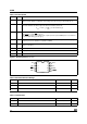
Table 1. Pin Description
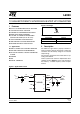
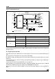
Figure 2. Pin Connection (Top view)
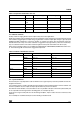
Table 2. Absolute Maximum Ratings
Table 3. Thermal Data
Pin Name Function
1FB
Output voltage selector. Connect FB to GND for Vout=5V or to OUT for Vout=3.3V. Connect FB to an
external resistor divider for adjustable output voltage (from 2V to 5.2V) [see R4 and R5, fig. 7].
2 LBI Battery low voltage detector input. The internal threshold is set to 1.23V.
A resistor divider is needed to adjust the desired low battery threshold:
[see R1 and R2, fig. 7]
3
LBO
Battery low voltage detector output. If the voltage at the LBI pin drops below the internal
threshold typ. 1.23V, LBO goes low.
The
LBO is an open drain output and so a pull-up resistor (about 200KΩ) has to be added for
correct output setting [see R3, fig. 7].
4 REF 1.23V reference voltage. Bypass this output to GND with a 100nF capacitor for filtering high
frequency noise. No capacitor is required for stability
5
SHDN
Shutdown pin. When pin 5 is below 0.2V the device is in shutdown, when pin 5 is above 0.6V the
device is operating.
6 GND Ground pin
7 LX Step-up inductor connection
8 OUT Power OUTPUT pin
Symbol Parameter Value Unit
V
ccmax
V
cc
to GND 6 V
LBI, SHDN, FB to GND 6 V
V
out max
Vout to GND 6 V
Symbol Parameter Value Unit
R
th j-amb
Thermal Resistance Junction to Ambient 250 °C/W
T
j
Maximum Junction Temperature 150 °C
V
LBI
1.23V= 1
R1
R2
------- -+
⎝⎠
⎛⎞
⋅
FB
LBI
REF
GND
LX
OUT1
3
2
4
6
5
7
8
TSSOP
8
LBO
SHDN