
Datasheet


Electrical characteristics LD1117A
8/24 DocID7194 Rev 26
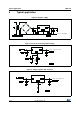
Refer to the test circuits, T
J
= 0 to 125 °C, C
O
= 10 µF, C
I
= 10 µF, unless otherwise
specified.
Refer to the test circuits, T
J
= 0 to 125 °C, C
O
= 10 µF, C
I
= 10 µF, unless otherwise
specified.
eN Output noise voltage B = 10 Hz to 10 kHz, T
J
= 25 °C 100 µV
SVR Supply voltage rejection
I
O
= 40 mA, f = 120 Hz
V
I
- V
O
= 3 V, V
ripple
= 1 V
PP
60 80 dB
V
D
Dropout voltage
I
O
= 100 mA 1 1.10
VI
O
= 500 mA 1.05 1.15
I
O
= 1 A 1.15 1.30
ΔV
O(pwr)
Thermal regulation T
a
= 25 °C, 30 ms pulse 0.08 0.2 %/W
Table 5. Electrical characteristics of LD1117A#18 (continued)
Symbol Parameter Test conditions Min. Typ. Max. Unit
Table 6. Electrical characteristics of LD1117A#33
Symbol Parameter Test conditions Min. Typ. Max. Unit
V
O
Output voltage V
I
= 5.3 V, I
O
= 10 mA, T
J
= 25 °C 3.234 3.3 3.366 V
V
O
Output voltage I
O
= 0 to 1 A, V
I
= 4.75 to 10 V 3.168 3.432 V
ΔV
O
Line regulation V
I
= 4.75 to 8 V, I
O
= 0 mA 1 6 mV
ΔV
O
Load regulation V
I
= 4.75 V, I
O
= 0 to 1 A 1 10 mV
ΔV
O
Temperature stability 0.5 %
ΔV
O
Long term stability 1000 hrs, T
J
= 125 °C 0.3 %
V
I
Operating input voltage I
O
= 100 mA 10 V
I
d
Quiescent current V
I
≤ 10 V, I
O
= 0 mA 5 10 mA
I
O
Output current V
I
- V
O
= 5 V, T
J
= 25 °C 1000 1200 mA
eN Output noise voltage B =10 Hz to 10 kHz, T
J
= 25 °C 100 µV
SVR Supply voltage rejection
I
O
= 40 mA, f = 120 Hz
V
I
- V
O
= 3 V, V
ripple
= 1 V
PP
60 75 dB
V
D
Dropout voltage
I
O
= 100 mA 1 1.10
VI
O
= 500 mA 1.05 1.15
I
O
= 1 A 1.15 1.30
ΔV
O(pwr)
Thermal regulation T
a
= 25 °C, 30 ms pulse 0.08 0.2 %/W
Table 7. Electrical characteristics of LD1117A (adjustable)
Symbol Parameter Test conditions Min. Typ. Max. Unit
V
REF
Reference voltage V
I
= 5.3 V, I
O
= 10 mA, T
J
= 25 °C 1.225 1.25 1.275 V
V
REF
Reference voltage I
O
= 10 mA to 1 A, V
I
= 2.75 to 10 V 1.2 1.3 V
ΔV
O
Line regulation V
I
= 2.75 to 8 V, I
O
= 0 mA 1 6 mV