LM124, LM224, LM324 Low power quad operational amplifiers Features ■ Wide gain bandwidth: 1.3 MHz ■ Input common-mode voltage range includes ground ■ Large voltage gain: 100 dB ■ Very low supply current per amplifier: 375 µA ■ Low input bias current: 20 nA ■ Low input offset voltage: 5 mV max. ■ Low input offset current: 2 nA ■ Wide power supply range: – Single supply: +3 V to +30 V ■ Dual supplies: ±1.
Pin and schematic diagram 1 LM124, LM224, LM324 Pin and schematic diagram Figure 1. Pin connections (top view) 14 Output 4 Output 1 1 Inverting Input 1 2 - - 13 Inverting Input 4 Non-inverting Input 1 3 + + 12 Non-inverting Input 4 11 VCC - VCC + 4 Non-inverting Input 2 Inverting Input 2 5 + + 10 Non-inverting Input 3 6 - - 9 Inverting Input 3 8 Output 3 Output 2 7 OUT1 OUT4 IN4- 16 15 14 13 2/19 IN1- Figure 2.
LM124, LM224, LM324 Absolute maximum ratings 2 Absolute maximum ratings Table 1. Absolute maximum ratings Symbol VCC Vin Vid Parameter LM124 LM224 Supply voltage Input voltage (1) Differential input voltage Unit ±16 or 32 V -0.3 to 32 V 32 V (2) Output short-circuit duration (3) LM324 Infinite (4) 5 mA in DC or 50 mA in AC (duty cycle = 10%, T=1s) Input current : Vin driven negative Input current (5): Vin driven positive above AMR value 0.
Electrical characteristics 3 LM124, LM224, LM324 Electrical characteristics Table 2. VCC+ = +5 V, VCC-= ground, Vo = 1.4 V, Tamb = +25° C (unless otherwise specified) Symbol Vio Parameter Min. Input offset voltage (1) Tamb = +25° C LM124-LM224 LM324 Typ. Max.
LM124, LM224, LM324 Table 2. Electrical characteristics VCC+ = +5 V, VCC-= ground, Vo = 1.4 V, Tamb = +25° C (unless otherwise specified) (continued) Symbol Isink VOH Parameter Min. Typ. Output sink current (Vid = -1 V) VCC = +15 V, Vo = +2 V VCC = +15 V, Vo = +0.2 V 10 12 20 50 High level output voltage VCC = +30 V Tamb = +25° C, RL = 2 kΩ Tmin ≤ Tamb ≤ Tmax Tamb = +25° C, RL = 10 kΩ Tmin ≤ Tamb ≤ Tmax 26 26 27 27 27 VCC = +5 V, RL = 2 kΩ Tamb = +25°C Tmin ≤ Tamb ≤ Tmax 3.5 3 Max.
Electrical characteristics Figure 3. LM124, LM224, LM324 Input bias current vs. ambient temperature Figure 4. Current limiting 90 IB (nA) 24 80 18 70 Input current (mA) 21 15 12 9 6 3 IO + 60 50 40 30 20 10 0 -55-35-15 0 5 25 45 65 85 105 125 -55 -35 -15 5 Ambient temperature (°C) Figure 5. Temperature (°C) Input voltage range Figure 6.
LM124, LM224, LM324 Figure 9. Electrical characteristics Open loop frequency response 140 Figure 10. Large signal frequency response 20 10 MΩ 100 kΩ 0.1 uF 1 kΩ 120 VCC+ VCC+/2 80 VCC+ = +30 V & -55°C Tamb +125°C 60 40 VCC+ = +10 to +15 V & -55°C Tamb +125°C 20 10 5 0 1.0 100 1.0k 10k 100k 1.0M 10M 10 1k 10k Frequency (Hz) 1M 100k Frequency (Hz) Figure 11. Voltage follower pulse response Figure 12.
Electrical characteristics LM124, LM224, LM324 Figure 15. Input current Figure 16. Large signal voltage gain Avd (dB) 100 Large signal voltage gain 120 Input current (nA) 75 50 Tamb = +25°C 25 20 110 105 100 -55 -35 -15 0 10 115 30 Figure 17. Power supply and common mode rejection ratio 160 115 SVR 110 RL = 20 kΩ 120 105 100 95 90 85 80 CMR Voltage gain (dB) Power supply & common mode rejection ratio (dB) 25 45 65 80 105 125 Figure 18.
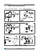
LM124, LM224, LM324 4 Typical single-supply applications Typical single-supply applications Figure 19. AC coupled inverting amplifier Figure 20. High input Z adjustable gain DC instrumentation amplifier 2 Vpp if R1 = R5 and R3 = R4 = R6 = R7 2R e0 = 1 + ----------1- (e2 -e1) R 2 Figure 21. AC coupled non inverting amplifier Figure 22. DC summing amplifier 2 Vpp e0 = e1 +e2 -e3 -e4 Where (e1 +e2) ≥ (e3 +e4) to keep e0 ≥ 0V Figure 23. Non-inverting DC gain Figure 24.
Typical single-supply applications LM124, LM224, LM324 Figure 25. Active bandpass filter Figure 26. High input Z, DC differential amplifier R R 1 4 For ------- = ------R R 2 3 (CMRR depends on this resistor ratio match) Fo = 1kHz Q = 50 Av = 100 (40dB) e0 (e2 - e1) As shown e0 = (e2 - e1) Figure 27.
LM124, LM224, LM324 5 Package information Package information In order to meet environmental requirements, ST offers these devices in different grades of ECOPACK® packages, depending on their level of environmental compliance. ECOPACK® specifications, grade definitions and product status are available at: www.st.com. ECOPACK® is an ST trademark.
Package information 5.1 LM124, LM224, LM324 DIP14 package information Figure 28. DIP14 package mechanical drawing Table 3. DIP14 package mechanical data Dimensions Millimeters Inches Ref. Min. Typ. A Min. Typ. 5.33 Max. 0.21 A1 0.38 0.015 A2 2.92 3.30 4.95 0.11 0.13 0.19 b 0.36 0.46 0.56 0.014 0.018 0.022 b2 1.14 1.52 1.78 0.04 0.06 0.07 c 0.20 0.25 0.36 0.007 0.009 0.01 D 18.67 19.05 19.69 0.73 0.75 0.77 E 7.62 7.87 8.26 0.30 0.31 0.32 E1 6.10 6.
LM124, LM224, LM324 5.2 Package information SO-14 package information Figure 29. SO-14 package mechanical drawing Table 4. SO-14 package mechanical data Dimensions Millimeters Inches Ref. Min. Typ. Max. Min. Typ. Max. A 1.35 1.75 0.05 0.068 A1 0.10 0.25 0.004 0.009 A2 1.10 1.65 0.04 0.06 B 0.33 0.51 0.01 0.02 C 0.19 0.25 0.007 0.009 D 8.55 8.75 0.33 0.34 E 3.80 4.0 0.15 0.15 e 1.27 0.05 H 5.80 6.20 0.22 0.24 h 0.25 0.50 0.009 0.02 L 0.40 1.
Package information 5.3 LM124, LM224, LM324 QFN16 3x3 package mechanical data Figure 30.
LM124, LM224, LM324 Table 5. Package information QFN16 3x3 mm package mechanical data (pitch 0.5 mm) Dimensions Ref. Millimeters Inches Min. Typ. Max. Min. Typ. Max. A 0.80 0.90 1.00 0.031 0.035 0.039 A1 0 0.05 0 A3 0.20 b 0.18 D 2.90 D2 1.50 E 2.90 E2 1.50 e L 3.00 3.00 0.008 0.30 0.007 3.10 0.114 1.80 0.059 3.10 0.114 1.80 0.059 0.50 0.30 0.002 0.012 0.118 0.122 0.071 0.118 0.122 0.071 0.020 0.50 0.012 0.020 Figure 31.
Package information 5.4 LM124, LM224, LM324 TSSOP14 package information Figure 32. TSSOP14 package mechanical drawing Figure 33. TSSOP14 package mechanical data Dimensions Ref. Millimeters Min. Typ. A Max. Min. Typ. 1.20 A1 0.05 A2 0.80 b Max. 0.047 0.15 0.002 0.004 0.006 1.05 0.031 0.039 0.041 0.19 0.30 0.007 0.012 c 0.09 0.20 0.004 0.0089 D 4.90 5.00 5.10 0.193 0.197 0.201 E 6.20 6.40 6.60 0.244 0.252 0.260 E1 4.30 4.40 4.50 0.169 0.173 0.
LM124, LM224, LM324 Ordering information 6 Ordering information Table 6.
Revision history 7 LM124, LM224, LM324 Revision history 0 Table 7. Document revision history Date Revision 01-Oct.-2003 1 First release. 02-Jan-2005 2 Modifications on AMR Table 1 on page 3 (explanation of Vid and Vi limits). 01-Jun-2005 3 ESD protection inserted in Table 1 on page 3. 02-Jan-2006 4 Tj and Rthjc parameters added in Table 1. on page 3. 04-Oct-2006 5 Editorial update. Table 3 moved to Section 5: Macromodels on page 11.
LM124, LM224, LM324 Please Read Carefully: Information in this document is provided solely in connection with ST products. STMicroelectronics NV and its subsidiaries (“ST”) reserve the right to make changes, corrections, modifications or improvements, to this document, and the products and services described herein at any time, without notice. All ST products are sold pursuant to ST’s terms and conditions of sale.