
Datasheet


LMV331, LMV393, LMV339 Electrical characteristics
Doc ID 16866 Rev 3 5/17
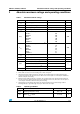
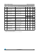
Table 4. V
CC
+
=+5V, V
CC
-
= 0 V, T
amb
= +25°C, full V
ICM
range (unless otherwise specified)
(1)
Symbol Parameter Test conditions Min. Typ. Max. Unit
V
IO
Input offset voltage
-40°C < T
amb
< +85°C
17
9
mV
ΔV
IO
Input offset voltage drift -40°C < T
amb
< +85°C 5 μV/°C
I
IB
Input bias current
(2)
-40°C < T
amb
< +85°C
25 250
400
nA
I
IO
Input offset current
(2)
-40°C < T
amb
< +85°C
250
150
nA
V
ICM
Common mode input voltage
-0.1
V
4.2
A
V
Voltage gain 20 50 V/mV
V
OL
Output voltage low
I
SINK
< 4 mA
-40°C < T
amb
< +85°C
50 400
700
mV
I
SINK
Output sink current V
OUT
< 1.5 V 10 93 mA
I
CC
Supply current
No load, output high, V
ICM
= 0 V
-40°C < T
amb
< +85°C
25 120
150
μA
I
OH
Output current leakage
-40°C < T
amb
< +85°C
0.003
1
μA
TP
HL
Propagation delay
High to low output level
V
ICM
= 0 V, R
L
= 5.1 kΩ, C
L
= 50 pF
Overdrive = 10 mV
Overdrive = 100 mV
375
275
ns
TP
LH
Propagation delay
Low to high output level
V
ICM
= 0 V, R
L
= 5.1 kΩ, C
L
= 50 pF
Overdrive = 10 mV
Overdrive = 100 mV
550
425
ns
1. All values over the temperature range are guaranteed through correlation and simulation. No production tests have been
performed at the temperature range limits.
2. Maximum values include unavoidable inaccuracies of the industrial tests.