
Datasheet


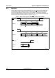
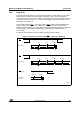
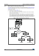
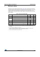
Table Of Contents
- 1 Description
- 2 Signal description
- 3 Memory organization
- 4 Device operation
- 5 Instructions
- 6 Initial delivery state
- 7 Maximum rating
- 8 DC and AC parameters
- Table 5. Operating conditions (voltage range W)
- Table 6. Operating conditions (voltage range R)
- Table 7. Operating conditions (voltage range F, for devices identified by process letter T)
- Table 8. Operating conditions (voltage range F, for all other devices)
- Table 9. AC measurement conditions
- Figure 9. AC measurement I/O waveform
- Table 10. Input parameters
- Table 11. Cycling performance
- Table 12. Memory cell data retention
- Table 13. DC characteristics (M24C01/02-W, device grade 6)
- Table 14. DC characteristics (M24C01/02-R, device grade 6)
- Table 15. DC characteristics (M24C02-F, device grade 6)
- Table 16. 400 kHz AC characteristics
- Table 17. 100 kHz AC characteristics (I2C Standard mode)
- Figure 10. Maximum Rbus value versus bus parasitic capacitance (Cbus) for an I2C bus at maximum frequency fC = 400 kHz
- Figure 11. AC waveforms
- 9 Package mechanical data
- Figure 12. TSSOP8 – 8-lead thin shrink small outline, package outline
- Table 18. TSSOP8 – 8-lead thin shrink small outline, package mechanical data
- Figure 13. SO8N – 8-lead plastic small outline, 150 mils body width, package outline
- Table 19. SO8N – 8-lead plastic small outline, 150 mils body width, package data
- Figure 14. PDIP8 – 8-pin plastic DIP, 0.25 mm lead frame, package outline
- Table 20. PDIP8 – 8-pin plastic DIP, 0.25 mm lead frame, package mechanical data
- Figure 15. UFDFPN8 (MLP8) – package outline (UFDFPN: Ultra thin Fine pitch Dual Flat Package, No lead)
- Table 21. UFDFPN8 (MLP8) – package dimensions (UFDFPN: Ultra thin Fine pitch Dual Flat Package, No lead)
- 10 Part numbering
- 11 Revision history
DC and AC parameters M24C01/02-W M24C01/02-R M24C02-F
20/34 DocID024020 Rev 2
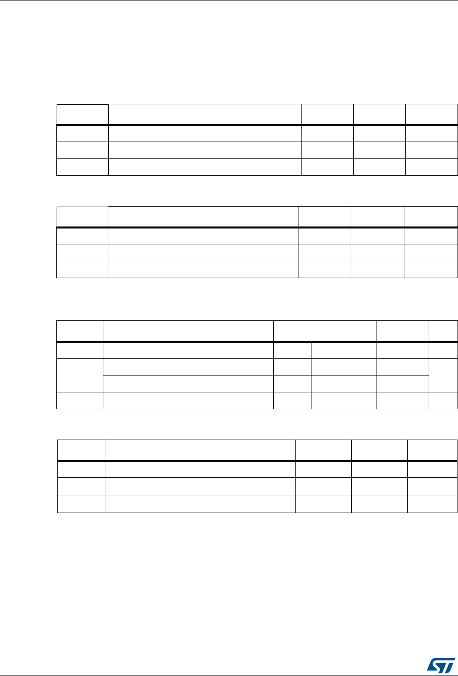
8 DC and AC parameters
This section summarizes the operating and measurement conditions, and the DC and AC
characteristics of the device.
Table 5. Operating conditions (voltage range W)
Symbol Parameter Min. Max. Unit
V
CC
Supply voltage 2.5 5.5 V
T
A
Ambient operating temperature –40 85 °C
f
C
Operating clock frequency - 400 kHz
Table 6. Operating conditions (voltage range R)
Symbol Parameter Min. Max. Unit
V
CC
Supply voltage 1.8 5.5 V
T
A
Ambient operating temperature –40 85 °C
f
C
Operating clock frequency - 400 kHz
Table 7. Operating conditions (voltage range F,
for devices identified by process letter T)
Symbol Parameter Min. Max. U
nit
V
CC
Supply voltage 1.60 1.65 1.70 5.5 V
T
A
Ambient operating temperature: READ -40 -40 -40 85
°C
Ambient operating temperature: WRITE 0 -20 -40 85
f
C
Operating clock frequency - - - 400 kHz
Table 8. Operating conditions (voltage range F, for all other devices)
Symbol Parameter Min. Max. U
nit
V
CC
Supply voltage 1.7 5.5 V
T
A
Ambient operating temperature -20 85 °C
f
C
Operating clock frequency - 400 kHz