
Datasheet

M74HC02
3/8
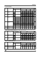
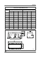
DC SPECIFICATIONS
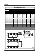
AC ELECTRICAL CHARACTERISTICS (C
L
= 50 pF, Input t
r
= t
f
= 6ns)
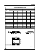
CAPACITIVE CHARACTERISTICS
1) C
PD
is defined as the value of the IC’s internal equivalent capacitance which is calculated from the operating current consumption without
load. (Refer to Test Circuit). Average operating current can be obtained by the following equation. I
CC(opr)
= C
PD
x V
CC
x f
IN
+ I
CC
/4 (per gate)
Symbol Parameter
Test Condition Value
Unit
V
CC
(V)
T
A
= 25°C
-40 to 85°C -55 to 125°C
Min. Typ. Max. Min. Max. Min. Max.
V
IH
High Level Input
Voltage
2.0 1.5 1.5 1.5
V4.5 3.15 3.15 3.15
6.0 4.2 4.2 4.2
V
IL
Low Level Input
Voltage
2.0 0.5 0.5 0.5
V4.5 1.35 1.35 1.35
6.0 1.8 1.8 1.8
V
OH
High Level Output
Voltage
2.0
I
O
=-20 µA
1.9 2.0 1.9 1.9
V
4.5
I
O
=-20 µA
4.4 4.5 4.4 4.4
6.0
I
O
=-20 µA
5.9 6.0 5.9 5.9
4.5
I
O
=-4.0 mA
4.18 4.31 4.13 4.10
6.0
I
O
=-5.2 mA
5.68 5.8 5.63 5.60
V
OL
Low Level Output
Voltage
2.0
I
O
=20 µA
0.0 0.1 0.1 0.1
V
4.5
I
O
=20 µA
0.0 0.1 0.1 0.1
6.0
I
O
=20 µA
0.0 0.1 0.1 0.1
4.5
I
O
=4.0 mA
0.17 0.26 0.33 0.40
6.0
I
O
=5.2 mA
0.18 0.26 0.33 0.40
I
I
Input Leakage
Current
6.0
V
I
= V
CC
or GND
± 0.1 ± 1 ± 1 µA
I
CC
Quiescent Supply
Current
6.0
V
I
= V
CC
or GND
11020µA
Symbol Parameter
Test Condition Value
Unit
V
CC
(V)
T
A
= 25°C
-40 to 85°C -55 to 125°C
Min. Typ. Max. Min. Max. Min. Max.
t
TLH
t
THL
Output Transition
Time
2.0 30 75 95 110
ns4.5 8151922
6.0 7131619
t
PLH
t
PHL
Propagation Delay
Time
2.0 27 75 95 110
ns4.5 9151922
6.0 8131619
Symbol Parameter
Test Condition Value
Unit
V
CC
(V)
T
A
= 25°C
-40 to 85°C -55 to 125°C
Min. Typ. Max. Min. Max. Min. Max.
C
IN
Input Capacitance
5.0 5101010pF
C
PD
Power Dissipation
Capacitance (note
1)
5.0 21 pF