
Product Card
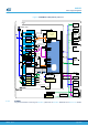

6.12.1 NAND IO interface
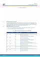
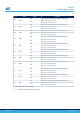
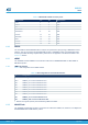
Table 15 features the HW configuration for the NAND interface.
T
able 15. HW configuration for the Quad-SPI interface
IO
Configuration
(1)
PD6 NAND_NWAIT connected to MB1262/U11 R/B#
PD11 NAND_CLE connected to MB1262/U11 CLE
PD12 NAND_ALE connected to MB1262/U11 ALE
PG9 NAND_NCE connected to MB1262/U11 CE#
PD5 NAND_NWE connected to MB1262/U11 WE#
PD4 NAND_NOE connected to MB1262/U11 RE#
PD14 NAND_D0 connected to MB1262/U11 IO0
PD15 NAND_D1 connected to MB1262/U11 IO1
PD0 NAND_D2 connected to MB1262/U11 IO2
PD1 NAND_D3 connected to MB1262/U11 IO3
PE7 NAND_D4 connected to MB1262/U11 IO4
PE8 NAND_D5 connected to MB1262/U11 IO5
PE9 NAND_D6 connected to MB1262/U11 IO6
PE10 NAND_D7 connected to MB1262/U11 IO7
1.
Minimum set of signals required by the boot ROM during NAND boot in bold
6.13 Quad-SPI NOR Flash
The STM32MP157xAA3 Quad-SPI interface is in dual-Serial mode to interface with two NOR Flash memories in
parallel. T
wo MX25L51245G-XD, 3V3/512-Mbit each, are fitted on the STM32MP157x-EV1 MB1262, in
MB1262/U14 and MB1262/U15 positions.
6.13.1 Quad-SPI IO interface
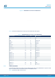
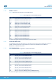
Table 16 describes the HW configuration for the Quad-SPI interface
T
able 16. HW configuration for the Quad-SPI interface
IO
Configuration
(1)
PF8 QSPI_BK1_IO0 connected to MB1262/U14 SIO0
PF9 QSPI_BK1_IO1 connected to MB1262/U14 SIO1
PF7 QSPI_BK1_IO2 connected to MB1262/U14 SIO2
PF6 QSPI_BK1_IO3 connected to MB1262/U14 SIO3
PB6 QSPI_BK1_NCS connected to MB1262/U14 CS#
PH2 QSPI_BK2_IO0 connected to MB1262/U15 SIO0
PH3 QSPI_BK2_IO1 connected to MB1262/U15 SIO1
PG10 QSPI_BK2_IO2 connected to MB1262/U15 SIO2
PG7 QSPI_BK2_IO3 connected to MB1262/U15 SIO3
PC0 QSPI_BK2_NCS connected to MB1262/U15 CS#
PF10 QSPI_CLK connected to MB1262/U14 SCLK and MB1262/U15 SCLK
1.
Minimum set of signals required by the boot ROM during dual-serial NOR boot in bold
UM2535
Quad-SPI NOR Flash
UM2535 - Rev 2
page 21/59