
User's Manual
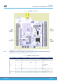
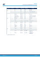
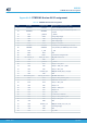
Table Of Contents
- 1 Features
- 2 Ordering information
- 3 Development environment
- 4 Conventions
- 5 Quick start
- 8 STM32WL Nucleo-64 board information
- Appendix A STM32WL Nucleo-64 I/O assignment
- Appendix B Federal Communications Commission (FCC) and Innovation, Science and Economic Development Canada (ISED) Compliance Statements
- Appendix C Déclaration de conformité CE simplifiée
- Revision history
- Contents
- List of tables
- List of figures

CN7 odd pins CN7 even pins CN10 odd pins CN10 even pins
Pin nbr Pin name Pin nbr
Pin name
(1)
Pin nbr
Pin name
(1)
Pin nbr Pin name
11 NC 12 IOREF 11 PA5 12 PC6
13
PA13
(3)
14 NRST 13 PA6 14 PC0
15
PA14
(3)
16 3V3 15 PA7 16 PA8
17 PA15 18 5V 17 PA4 18 NC
19 GND 20 GND 19 PA9 20 GND
21 NC 22 GND 21 PC2 22 PB0
23 PC13 24 VIN 23 PC1 24 NC
25 PC14 26 NC 25 PB10 26 PB9
27 PC15 28 PB1 27 PB8 28 PB15
29 NC 30 PB2 29 PB5 30 PB11
31 NC 32 PA10 31 PB3 32 AGND
33 VBAT 34 PB4 33 PB12 34 NC
35 NC 36 PB14 35 PB6
/ PA2 36 PA1
37 NC 38 PB13 37 PB6
/ PA3 38 PC3
1. Default configuration in bold.
2. 5V_USB_CHGR is the 5 V power from the STLINK-V3E USB connector that rises first. It rises before the 5 V rising on the
board.
3. PA13 and PA14 are shared with SWD signals connected to STLINK-V3E. It is not recommended to use them as I/O pins.
UM2592
CN7 and CN10 ST morpho connectors
UM2592 - Rev 1
page 37/49