
User's Manual
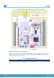
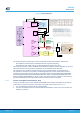
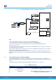
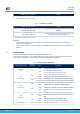
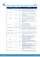
Table Of Contents
- 1 Features
- 2 Ordering information
- 3 Development environment
- 4 Conventions
- 5 Quick start
- 8 NUCLEO-WL55JC board information
- Appendix A STM32WL Nucleo-64 I/O assignment
- Appendix B Federal Communications Commission (FCC) and Innovation, Science and Economic Development Canada (ISED) Compliance Statements
- Appendix C Déclaration de conformité CE simplifiée
- Revision history
- Contents
- List of tables
- List of figures

Figure 19. JP1 and JP4 settings for current consumption measurement
RF part
MCU STM32WL
LDO
LD39050PU33R
5V
U2
JP4
5V_USB_STLK
5V_VIN
E5V
5V_USB_CHGR
VDD_MCU
(VDD_RF)
(VDD_SYS)
(VREF+)
JP1
ON
STD_ALONE_5V
TCXO
RF front-end
(PB0_VDD_TCXO)
VDD_RF
SB28 (ON)
VDD_SYS
SB27 (ON)
VDD_APP
SB32 (ON)
3V3
JP2 OFF
JP5 OFF
JP9 OFF
VBAT
VDD_SYS
SB21
(ON)
AVDD
SB26
(ON)
VDD_SYS
SB24
(ON)
(VBAT)
Note:
I_SoC (on VDD_MCU) is the current consumption of all the STM32WL MCU.
I_RF (on VDD_RF) is the current consumption of the RF part of the STM32WL MCU.
I_SYS (on VDD_SYS) is the current consumption of the rest of the STM32WL MCU (except I-RF).
So I_SoC = I_RF + I_SYS
We can evaluate the current consumption of the RF part of the STM32WL MCU by connecting an ammeter on
JP2. SB28 must be OFF in this case.
We can also evaluate the current consumption of the rest of the STM32WL MCU (VDD_SYS) by connecting an
ammeter on JP5. SB27 must be OFF in this case.
We can also evaluate the RF front-end current consumption (VDD_APP) by connecting an ammeter on JP9.
SB32 must be OFF in this case. This current consumption only concerns both NX3L1T3157GM DC switches (U3
and U4).
6.6.5 Virtual COM port (VCP): LPUART and USART
The STM32WL Nucleo-64 board offers the possibility to select which USART interface is connected to the
STLINK-V3E, ARDUINO
®
Uno V3 connector (CN9 pins 2 and 1), or to the ST morpho connector (CN10 pins 35
and 37).
The selection is done by setting the related solder bridges as detailed in Table 11 and Table 12.
Table 11. USART1 connection
Solder bridge configuration
(1)
Feature
(1)
SB6, SB10: ON
SB7, SB9, SB3, SB5: OFF
USART1 (PB6/PB7) connected to STLINK-V3E virtual COM
port.
SB7, SB9: ON
USART1 (PB6/PB7) connected to Arduino™ (D1 & D0) and
ST morpho connector (CN10 pin 35 and 37).
UM2592
Board functions
UM2592 - Rev 2
page 28/50