
Datasheet

DocID5257 Rev 11 5/23
MC34063AB, MC34063AC, MC34063EB, MC34063EC Maximum ratings
3 Maximum ratings
Note: Absolute maximum ratings are those values beyond which damage to the device may occur.
Functional operation under these condition is not implied.
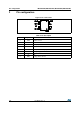
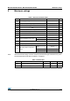
Table 3. Absolute maximum ratings
Symbol Parameter Value Unit
V
CC
Power supply voltage 50 V
V
IR
Comparator input voltage range -0.3 to 40 V
V
SWC
Switch collector voltage 40 V
V
SWE
Switch emitter voltage (V
SWC
= 40V) 40 V
V
CE
Switch collector to emitter voltage 40 V
V
DC
Driver collector voltage 40 V
I
DC
Driver collector current 100 mA
I
SW
Switch current 1.5 A
P
TOT
Power dissipation at T
A
= 25°C
for DIP-8 1.25
W
for SO-8 0.625
T
J
Operating junction temperature 150 °C
T
STG
Storage temperature range -40 to 150 °C
T
OP
Operating ambient temperature
range
for AC and EC
series
0 to 70
°C
for AB series -40 to 85
for EB series -40 to 125
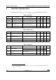
Table 4. Thermal data
Symbol Parameter DIP-8 SO-8 Unit
R
thJA
Thermal resistance junction-ambient
(1)
1. This value depends from thermal design of PCB on which the device is mounted.
100 160 °C/W
R
thJC
Thermal resistance junction-case 42 20 °C/W