
User's Manual

UM2252
Component description
DocID030806 Rev 2
17/26
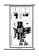
4.3 PCB Layout
4.3.1 PCB layers
As the ST25R3911B is a high power RF transmitter, the NFC reader layout must be done
carefully.
The decoupling capacitors are located as close as possible to the positive and negative
power supply pins (for example VSP_RF and VSN_RF).
Since the chip is using a differential output driver stage, the antenna matching network is
treated as a differential network.
The space between the components is kept as small as possible and the whole network is
routed completely symmetrical.
Via stitching and via shielding is used to maintain a low impedance and prevent short
return current loops.
The RF traces are protected by via stitching in combination with guard rings to create a via
wall: this keeps the PCB electromagnetically 'quiet'.
A via shield is used to create a vertical copper barrier through the PCB, to help reduce
crosstalk and electromagnetic interference in a route carrying an RF signal.
The RFI traces and AAT lanes are routed as close as possible to each other.
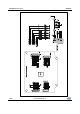
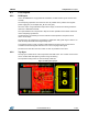
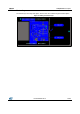
4.3.2 Top layer
The top layer contains most of the components and PCB traces. The unused areas around
the IC are filled with GND planes guarded using via stitching.
The important analog traces are surrounded by GND vias.
Figure 6: PCB layout top layer