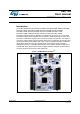
UM1724 User manual STM32 Nucleo-64 boards Introduction The STM32 Nucleo-64 board (NUCLEO-F030R8, NUCLEO-F070RB, NUCLEO-F072RB, NUCLEO-F091RC, NUCLEO-F103RB, NUCLEO-F302R8, NUCLEO-F303RE, NUCLEO-F334R8, NUCLEO-F401RE, NUCLEO-F410RB, NUCLEO-F411RE, NUCLEO-F446RE, NUCLEO-L053R8, NUCLEO-L073RZ, NUCLEO-L152RE, NUCLEO-L476RG) provides an affordable and flexible way for users to try out new ideas and build prototypes with the STM32 microcontrollers in LQFP64 package, choosing from the various combinations of perf
Content UM1724 Content 1 Ordering information . . . . . . . . . . . . . . . . . . . . . . . . . . . . . . . . . . . . . . . . 2 2 Conventions . . . . . . . . . . . . . . . . . . . . . . . . . . . . . . . . . . . . . . . . . . . . . . . 3 3 Quick start . . . . . . . . . . . . . . . . . . . . . . . . . . . . . . . . . . . . . . . . . . . . . . . . . 4 4 3.1 Getting started . . . . . . . . . . . . . . . . . . . . . . . . . . . . . . . . . . . . . . . . . . . . . . 4 3.2 System requirements . . . .
UM1724 Content 5.11 STMicroelectronics Morpho connector . . . . . . . . . . . . . . . . . . . . . . . . . . . 44 6 Mechanical drawing . . . . . . . . . . . . . . . . . . . . . . . . . . . . . . . . . . . . . . . . 53 7 Electrical schematics . . . . . . . . . . . . . . . . . . . . . . . . . . . . . . . . . . . . . . . 54 8 References . . . . . . . . . . . . . . . . . . . . . . . . . . . . . . . . . . . . . . . . . . . . . . . . 58 9 Revision history . . . . . . . . . . . . . . . . . . . . . . . .
List of Tables UM1724 List of Tables Table 1. Table 2. Table 3. Table 4. Table 5. Table 6. Table 7. Table 8. Table 9. Table 10. Table 11. Table 12. Table 13. Table 14. Table 15. Table 16. Table 17. Table 18. Table 19. Table 20. Table 21. Table 22. Table 23. Table 24. Table 25. Table 26. Table 27. Table 28. Table 29. Table 30. Table 31. 1/61 Ordering information . . . . . . . . . . . . . . . . . . . . . . . . . . . . . . . . . . . . . . . . . . . . . . . . . . . . . . . 2 ON/OFF conventions . . . . . . .
UM1724 List of Figures List of Figures Figure 1. Figure 1. Figure 2. Figure 3. Figure 4. Figure 5. Figure 6. Figure 7. Figure 8. Figure 9. Figure 10. Figure 11. Figure 12. Figure 13. Figure 14. Figure 15. Figure 16. Figure 17. Figure 18. Figure 19. Figure 20. Figure 21. Figure 22. Figure 23. Figure 24. Figure 25. Figure 26. Figure 27. Figure 28. STM32 Nucleo-64 board (1) . . . . . . . . . . . . . . . . . . . . . . . . . . . . . . . . . . . . . . . . . . . . . . . . . 1 Hardware block diagram . . . . . .
Ordering information 1 UM1724 Ordering information Table 1 lists the order codes and the respective targeted MCU. Table 1.
UM1724 2 Conventions Conventions Table 2 provides the conventions used for the ON and OFF settings in the present document. Table 2. ON/OFF conventions Convention Definition Jumper JP1 ON Jumper fitted Jumper JP1 OFF Jumper not fitted Solder bridge SBx ON SBx connections closed by solder or 0 ohm resistor Solder bridge SBx OFF SBx connections left open We refer to “STM32 Nucleo board” and “STM32 Nucleo boards” in this document for all information that is common to all sale types.
Quick start 3 UM1724 Quick start The STM32 Nucleo board is a low-cost and easy-to-use development platform used to quickly evaluate and start a development with an STM32 microcontroller in LQFP64 package. Before installing and using the product, please accept the Evaluation Product License Agreement from www.st.com/epla. For more information on the STM32 Nucleo boards and to access the demonstration software, visit www.st.com/stm32nucleo. 3.
UM1724 Quick start limitations to be worked around, as described hereunder. Parts with the date code starting from week 23 of 2015 contain bootloader V 9.2 in which the limitations no longer exist. To locate the visual date code information on the STM32L476RGT6 package, refer to its datasheet (DS10198) available on www.st.com, section Package Information. Date code related portion of the package marking takes Y WW format, where Y is the last digit of the year and WW is the week.
Features 4 UM1724 Features The STM32 Nucleo boards offer the following features: • STM32 microcontroller with LQFP64 package • Two types of extension resources – Arduino Uno Revision 3 connectivity – STMicroelectronics Morpho extension pin headers for full access to all STM32 I/Os • mbed-enabled(a) • On-board ST-LINK/V2-1 debugger/programmer with SWD connector – selection-mode switch to use the kit as a standalone ST-LINK/V2-1 • Flexible board power supply – USB VBUS – External VIN (7V
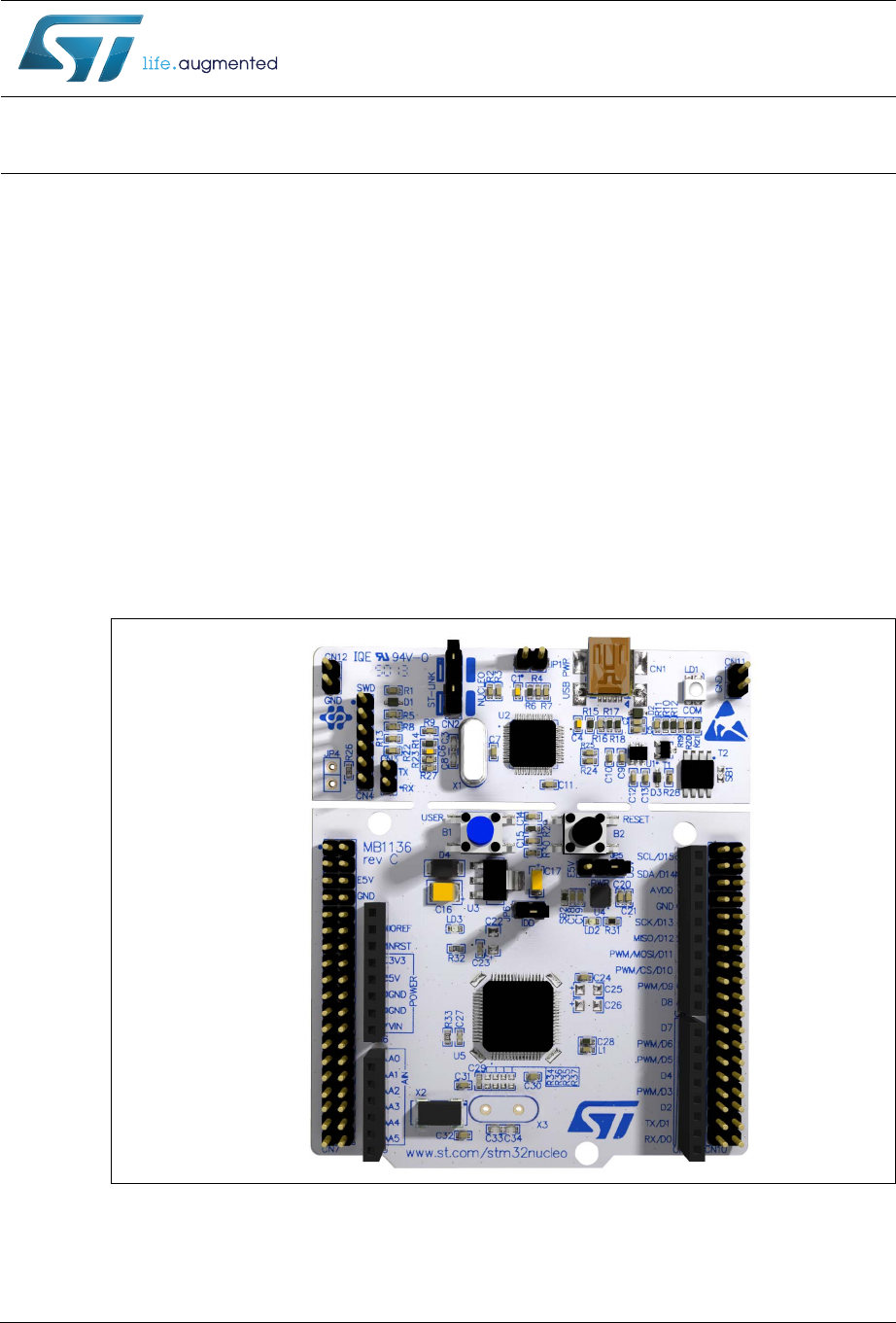
UM1724 Hardware layout and configuration The STM32 Nucleo board is designed around the STM32 microcontrollers in a 64-pin LQFP package. Figure 1 shows the connections between the STM32 and its peripherals (ST-LINK/V2-1, pushbutton, LED, Arduino connectors and STMicroelectronics Morpho connector). Figure 2 and Figure 3 show the location of these features on the STM32 Nucleo board. Figure 1. Hardware block diagram 67 /,1. SDUW 0LQL 86% (PEHGGHG 67 /,1.
Hardware layout and configuration UM1724 Figure 2. Top layout &1 67 /,1. 1XFOHR VHOHFWRU &1 6:' FRQQHFWRU &1 67 /,1. 86% PLQL % FRQQHFWRU /' 5HG *UHHQ /(' &20 % 5(6(7 EXWWRQ % 86(5 EXWWRQ -3 ,'' PHDVXUHPHQW 6% 9 UHJXODWRU RXWSXW /' 5HG /(' SRZHU /' *UHHQ /(' &1 $UGXLQR FRQQHFWRU &1 $UGXLQR FRQQHFWRU &1 67 0RUSKR FRQQHFWRU &1 $UGXLQR FRQQHFWRU &1 67 0RUSKR FRQQHFWRU &1 $UGXLQR FRQQHFWRU .
UM1724 Hardware layout and configuration Figure 3. Bottom layout 4# 4# 45 -*/, 64"35 4# 4# 4# 4# 3&4&37&% 4# 4# 4# 4# %&'"6-5 4# 45 -*/, 480 6% 67 /,1. 5(6(7 4# 45 -*/, .$0 6% 86(5 EXWWRQ 6% 86(5 /(' 6% 67 /,1. 0&2 .4 7 5.1 Cuttable PCB The STM32 Nucleo board is divided into two parts: ST-LINK part and target MCU part. The ST-LINK part of the PCB can be cut out to reduce the board size.
Hardware layout and configuration 5.2 UM1724 Embedded ST-LINK/V2-1 The ST-LINK/V2-1 programming and debugging tool is integrated in the STM32 Nucleo boards. The ST-LINK/V2-1 makes the STM32 Nucleo boards mbed enabled. The embedded ST-LINK/V2-1 supports only SWD for STM32 devices. For information about debugging and programming features refer to UM1075 - ST-LINK/V2 in-circuit debugger/programmer for STM8 and STM32, User manual, which describes in detail all the ST-LINK/V2 features.
UM1724 Hardware layout and configuration Figure 4. Typical configuration +DUGZDUH UHTXLUHPHQWV 86% FDEOH W\SH $ WR PLQL % FRPSXWHU ZLWK :LQGRZV ;3 'HYHORSPHQW WRROFKDLQ ,$5 (:$50 .HLO 0'. $50 *&& EDVHG ,'( 06 9 5.2.1 Driver The ST-LINK/V2-1 requires a dedicated USB driver, which can be found on www.st.com for Windows XP, 7, 8.
Hardware layout and configuration 5.2.3 UM1724 Using the ST-LINK/V2-1 to program/debug the STM32 on board To program the STM32 on the board, plug in the two jumpers on CN2, as shown in red in Figure 6. Do not use the CN4 connector as this could disturb the communication with the STM32 microcontroller of the STM32 Nucleo board. Figure 6. Connecting the STM32 Nucleo board to program the on-board STM32 EϮ ũƵŵƉĞƌƐ KE Eϰ ^t ĐŽŶŶĞĐƚŽƌ 06 9 5.2.
UM1724 Hardware layout and configuration Table 4. Debug connector CN4 (SWD) (continued) 5 NRST RESET of target MCU 6 SWO Reserved Figure 7. Using ST-LINK/V2-1 to program the STM32 on an external application $/ KVNQFST 0'' $/ 48% DPOOFDUPS .4 7 5.3 Power supply and power selection The power supply is provided either by the host PC through the USB cable, or by an external Source: VIN (7V-12V), E5V (5V) or +3V3 power supply pins on CN6 or CN7.
Hardware layout and configuration UM1724 All parts of the STM32 Nucleo board and shield can be powered from the ST-LINK USB connector CN1 (U5V or VBUS). Note that only the ST-LINK part is power supplied before the USB enumeration as the host PC only provides 100 mA to the board at that time. During the USB enumeration, the STM32 Nucleo board requires 300 mA of current to the Host PC.
UM1724 Hardware layout and configuration Table 6. External power sources Input power Connectors Voltage range name pins Max current Limitation VIN CN6 pin 8 CN7 pin 24 7 V to 12 V 800 mA From 7 V to 12 V only and input current capability is linked to input voltage: 800 mA input current when Vin=7 V 450 mA input current when 7 V
Hardware layout and configuration 16/61 UM1724 1. If more than 300 mA current is needed by the board, the PC may be damaged or the current supply can be limited by the PC. As a consequence the board is not powered correctly. 2. 300 mA is requested at enumeration (since JP1 must be OFF) so there is risk that the request is rejected and the enumeration does not succeed if the PC cannot provide such current. Consequently the board is not power supplied (LED LD3 remains OFF).
UM1724 5.3.3 Hardware layout and configuration External power supply input: + 3V3 It can be of interest to use the +3V3 (CN6 pin 4 or CN7 pin 12 and pin 16) directly as power input for instance in case the 3.3 V is provided by an extension board. When NUCLEO is power supplied by +3V3, the ST-LINK is not powered thus the programming and debug features are unavailable. The external power sources +3.3V is summarized in the Table 8. Table 8. +3.
Hardware layout and configuration 5.5 UM1724 Push buttons B1 USER: the user button is connected to the I/O PC13 (pin 2) of the STM32 microcontroller. B2 RESET: this push button is connected to NRST, and is used to RESET the STM32 microcontroller. Note: The blue and black plastic hats that are placed on the push buttons can be removed if necessary, for example when a shield or when an application board is plugged on top of NUCLEO.
UM1724 Hardware layout and configuration – • R35 and R37 removed HSE not used: PF0/PD0/PH1 and PF1/PD1/PH1 are used as GPIO instead of Clock The following configuration is needed: – SB54 and SB55 ON – SB16 and SB50 (MCO) OFF – R35 and R37 removed There are two possible default configurations of the HSE pins depending on the version of NUCLEO board hardware. The board version MB1136 C-01 or MB1136 C-02 is mentioned on sticker placed on bottom side of the PCB.
Hardware layout and configuration 5.7 UM1724 USART communication The USART2 interface available on PA2 and PA3 of the STM32 microcontroller can be connected to ST-LINK MCU, STMicroelectronics Morpho connector or to Arduino connector. The choice can be changed by setting the related solder bridges. By default the USART2 communication between the target MCU and ST-LINK MCU is enabled in order to support Virtual Com Port for mbed (SB13 and SB14 ON, SB62 and SB63 OFF).
UM1724 Hardware layout and configuration Table 9. Solder bridges (continued) Bridge SB2 (3.3 V) SB21 (LD2-LED) State ON Output of voltage regulator LD39050PU33R is connected to 3.3V. OFF Output of voltage regulator LD39050PU33R is not connected. ON Green user LED LD2 is connected to D13 of Arduino signal. OFF Green user LED LD2 is not connected. ON PC1 and PC0 (ADC in) are connected to A4 and A5 (pin 5 and pin 6) on Arduino connector CN8 and ST Morpho connector CN7.
Hardware layout and configuration UM1724 All STM32 Nucleo boards are delivered with the solder-bridges configured according to the target MCU supported. 5.9 Extension connectors The following figures show the signals connected by default to Arduino Uno Revision 3 connectors (CN5, CN6, CN8, CN9) and to STMicroelectronics Morpho connector (CN7 and CN10), for each STM32 Nucleo board. Figure 8.
UM1724 Hardware layout and configuration Figure 10.
Hardware layout and configuration UM1724 Figure 12.
UM1724 Hardware layout and configuration Figure 14.
Hardware layout and configuration UM1724 Figure 16.
UM1724 Hardware layout and configuration Figure 18.
Hardware layout and configuration UM1724 Figure 20.
UM1724 Hardware layout and configuration Figure 22.
Hardware layout and configuration 5.10 UM1724 Arduino connectors CN5, CN6, CN8 and CN9 are female connectors compatible with Arduino standard. Most shields designed for Arduino can fit to the STM32 Nucleo boards. The Arduino connectors on STM32 Nucleo board support the Arduino Uno Revision 3. For compatibility with Arduino Uno Revision 1, apply the following modifications: Caution: • SB46 and SB52 should be ON, • SB51 and SB56 should be OFF to connect I2C on A4 (pin 5) and A5 (pin 6 of CN8).
UM1724 Hardware layout and configuration Table 10. Arduino connectors on NUCLEO-F030R8, NUCLEO-F070RB, NUCLEO-F072RB, NUCLEO-F091RC (continued) CN No. Pin No.
Hardware layout and configuration UM1724 Table 11. Arduino connectors on NUCLEO-F103RB (continued) CN No. Pin No.
UM1724 Hardware layout and configuration Table 12. Arduino connectors on NUCLEO-F302R8 CN No. Pin No. Pin name MCU pin Function 1 NC - - 2 IOREF - 3.3V Ref 3 RESET NRST RESET 4 +3V3 - 3.
Hardware layout and configuration Warning: UM1724 PWM is not supported by D9 on STM32F302 since the timer is not available on PC7. Table 13. Arduino connectors on NUCLEO-F303RE CN No. Pin No. Pin name MCU pin Function 1 NC - - 2 IOREF - 3.3V Ref 3 RESET NRST RESET 4 +3V3 - 3.
UM1724 Hardware layout and configuration Table 13. Arduino connectors on NUCLEO-F303RE (continued) CN No. CN9 Digital Pin No. Pin name MCU pin Function 8 D7 PA8 - 7 D6 PB10 TIM2_CH3 6 D5 PB4 TIM3_CH1 5 D4 PB5 - 4 D3 PB3 TIM2_CH2 3 D2 PA10 - 2 D1 PA2 USART2_TX 1. Please refer to Table 9: Solder bridges or details. Table 14. Arduino connectors on NUCLEO-F334R8 CN No. Pin No. Pin name MCU pin Function 1 NC - - 2 IOREF - 3.
Hardware layout and configuration UM1724 Table 14. Arduino connectors on NUCLEO-F334R8 (continued) CN No. CN5 digital CN9 digital Pin No. Pin name MCU pin Function 1 D8 PA9 - 8 D7 PA8 - 7 D6 PB10 TIM2_CH3 6 D5 PB4 TIM3_CH1 5 D4 PB5 - 4 D3 PB3 TIM2_CH2 3 D2 PA10 - 2 D1 PA2 USART2_TX 1 D0 PA3 USART2_RX 1. Please refer to Table 9: Solder bridges for details. Table 15. Arduino connectors on NUCLEO-F401RE, NUCLEO-F411RE CN No. Pin No.
UM1724 Hardware layout and configuration Table 15. Arduino connectors on NUCLEO-F401RE, NUCLEO-F411RE (continued) CN No. CN5 digital CN9 digital Pin No. Pin name MCU pin Function 5 D12 PA6 SPI1_MISO 4 D11 PA7 TIM1_CH1N or SPI1_MOSI 3 D10 PB6 TIM4_CH1 or SPI1_CS 2 D9 PC7 TIM3_CH2 1 D8 PA9 - 8 D7 PA8 - 7 D6 PB10 TIM2_CH3 6 D5 PB4 TIM3_CH1 5 D4 PB5 - 4 D3 PB3 TIM2_CH2 3 D2 PA10 - 2 D1 PA2 USART2_TX 1 D0 PA3 USART2_RX 1.
Hardware layout and configuration UM1724 Table 16. Arduino connectors on NUCLEO-L053R8 (continued) Connect or No. CN5 digital CN9 digital Pin No.
UM1724 Hardware layout and configuration Table 17. Arduino connectors on NUCLEO-L073RZ (continued) CN No. CN8 analog Pin No.
Hardware layout and configuration UM1724 Table 18. Arduino connectors on NUCLEO-F446RE CN No. Pin No. Pin name MCU pin Function 1 NC - - 2 IOREF - 3.3V Ref 3 RESET NRST RESET 4 +3V3 - 3.
UM1724 Hardware layout and configuration Table 19. Arduino connectors on NUCLEO-F410RB CN No. Pin No. Pin name MCU pin Function 1 NC - - 2 IOREF - 3.3V Ref 3 RESET NRST RESET 4 +3V3 - 3.
Hardware layout and configuration UM1724 1. Please refer to Table 9: Solder bridges for details. Warning: PWM is not supported by D3, D5, D6, D9 and D10 on STM32F410RB since timer is not available on PB6, PC7, PB10, PB4, PB3. Table 20. Arduino connectors on NUCLEO-L152RE CN No. Pin No. Pin name MCU pin Function 1 NC - - 2 IOREF - 3.3V Ref 3 RESET NRST RESET 4 +3V3 - 3.
UM1724 Hardware layout and configuration Table 20. Arduino connectors on NUCLEO-L152RE (continued) CN No. CN9 digital Pin No. Pin name MCU pin Function 8 D7 PA8 - 7 D6 PB10 TIM2_CH3 6 D5 PB4 TIM3_CH1 5 D4 PB5 - 4 D3 PB3 TIM2_CH2 3 D2 PA10 - 2 D1 PA2 USART2_TX 1 D0 PA3 USART2_RX 1. Please refer to Table 9: Solder bridges for details. Table 21. Arduino connectors on NUCLEO-L476RG CN No. Pin No. Pin name MCU pin Function 1 NC - - 2 IOREF - 3.
Hardware layout and configuration UM1724 Table 21. Arduino connectors on NUCLEO-L476RG (continued) CN No. Pin No. Pin name MCU pin Function CN5 digital 2 D9 PC7 TIM3_CH2 1 D8 PA9 - 8 D7 PA8 - 7 D6 PB10 TIM2_CH3 6 D5 PB4 TIM3_CH1 5 D4 PB5 - 4 D3 PB3 TIM2_CH2 3 D2 PA10 - 2 D1 PA2 USART2_TX 1 D0 PA3 USART2_RX CN9 digital 1. Please refer to Table 9: Solder bridges for details. 5.
UM1724 Hardware layout and configuration Table 22. STMicroelectronics Morpho connector on NUCLEO-F030R8 (continued) CN7 odd pins CN7 even pins CN10 odd pins CN10 even pins Pin No. Name Name Pin No. Pin No. Name Name Pin No.
Hardware layout and configuration UM1724 Table 23. STMicroelectronics Morpho connector on NUCLEO-F070RB (continued) CN7 odd pins CN7 even pins CN10 odd pins CN10 even pins Pin No. Name Name Pin No. Pin No. Name Name Pin No. 35 PC2 PC1 or PB9(4) 36 35 PA2 - 36 37 PC3 PC0 or PB8(4) 38 37 PA3 - 38 1. Default state of BOOT0 is 0. It can be set to 1 when a jumper is on pin5-7 of CN7. 2. U5V is 5 V power from ST-LINK/V2-1 USB connector and it rises before +5V. 3.
UM1724 Hardware layout and configuration 3. U5V is 5 V power from ST-LINK/V2-1 USB connector and it rises before +5V. 4. PA13 and PA14 share with SWD signals connected to ST-LINK/V2-1, it is not recommended to use them as IO pins if ST-LINK part is not cut. 5. Please refer to Table 9: Solder bridges for detail. Table 25. STMicroelectronics Morpho connector on NUCLEO-F103RB CN7 odd pins CN7 even pins CN10 odd pins CN10 even pins Pin No. Name Name Pin No. Pin No. Name Name Pin No.
Hardware layout and configuration UM1724 Table 26. STMicroelectronics Morpho connector on NUCLEO-F302R8 CN7 odd pins CN7 even pins CN10 odd pins CN10 even pins Pin No. Name Name Pin No. Pin No. Name Name Pin No.
UM1724 Hardware layout and configuration Table 27. STMicroelectronics Morpho connector on NUCLEO-F401RE, NUCLEO-F411RE,NUCLEO-F446RE CN7 odd pins CN7 even pins CN10 odd pins CN10 even pins Pin No. Name Name Pin No. Pin No. Name Name Pin No.
Hardware layout and configuration UM1724 Table 28. STMicroelectronics Morpho connector on NUCLEO-L053R8, NUCLEO-L073RZ, NUCLEO-L152RE CN7 odd pins CN7 even pins CN10 odd pins CN10 even pins Pin No. Name Name Pin No. Pin No. Name Name Pin No.
UM1724 Hardware layout and configuration Table 29. STMicroelectronics Morpho connector on NUCLEO-L476RG CN7 odd pins CN7 even pins CN10 odd pins CN10 even pins Pin No. Name Name Pin No. Pin No. Name Name Pin No.
Hardware layout and configuration UM1724 Table 30. STMicroelectronics Morpho connector on NUCLEO-F410RB CN7 odd pins CN7 even pins CN10 odd pins CN10 even pins Pin No. Name Name Pin No. Pin No. Name Name Pin No.
UM1724 6 Mechanical drawing Mechanical drawing Figure 24.
Electrical schematics Electrical schematics 54/61 7 Figure 25 to Figure 28 show the electrical schematics of the STM32 Nucleo board. Figure 25. Electrical schematics (1/4) U_Connectors Connectors.SchDoc U_MCU_64 MCU_64.SchDoc PA[0..15] PB[0..15] PC[0..15] PD2 PD8 PF[0..1] PF[4..7] BOOT0 NRST PA[0..15] PB[0..15] PC[0..15] PD2 PD8 PF[0..1] PF[4..7] BOOT0 U_ST_LINK_V2-1 ST_LINK_V2-1.
UM1724 Figure 26. Electrical schematics (2/4) U5A PD8 PD8 PF[0..1] PF[4..7] A5 A4 PC0 PC1 PC2 PC3 PC4 PC5 PC6 PC7 8 9 10 11 24 25 37 38 TMS TCK PF[0..1] PF[4..
E5V SB15 PWR_EXT R1 SWD 48 47 46 45 44 43 42 41 40 39 38 37 8MHz(12pF) OSC_IN OSC_OUT STM_RST R23 AIN_1 4K7 VDD_3 VSS_3 PB9 PB8 BOOT0 PB7 PB6 PB5 PB4/JNTRST PB3/JTDO PA15/JTDI JTCK/SWCLK 36 35 34 33 32 31 30 29 28 27 26 25 +3V3_ST_LINK STM_JTMS USB_DP USB_DM T_SWO LED_STLINK 22 T_JTCK R8 22 T_JTMS R13 22 T_NRST R22 22 Header 6X1 SB4 SB5 SB6 SB7 SB8 SB9 SB10 MCO SB16 Default: closed Open for L476RG MCO PWR_ENn CN3 STLINK_RX SWCLK STM_JTMS SWDIO CN2 Jumpers ON --> NUCLEO
PA[0..15] PB[0..15] PC[0..15] PD2 PA[0..15] Extension connectors PB[0..15] SB20,SB24,SB29 Close only for F302R8 PC[0..15] BOOT0 PF[0..1] VDD NRST BOOT0 PF6 PF7 PA13 PA14 PA15 BOOT0 PB7 PC13 PF[4..
References 8 UM1724 References 1.
UM1724 9 Revision history Revision history Table 31. Document revision history Date Revision 10-Feb-2014 1 Initial release. 13-Feb-2014 2 Updated Figure 1, Chapter 4 and Table 9. 3 Extended the applicability to NUCLEO-F302R8. Updated Table 1: Ordering information, Section 5.10: Arduino connectors and Section 5.11: STMicroelectronics Morpho connector. Updated Figure 1 4 Updated the board figure: Figure 1. Updated HSE and LSE configuration description: Section 5.6.1, Section 4 and Section 5.6.2.
Revision history UM1724 Table 31. Document revision history (continued) Date 19-Jan-2015 Revision Changes 7 Extended the applicability to NUCLEO-F070RB, NUCLEOL073RZ and NUCLEO-L476RG; Updated Table 1: Ordering information; Updated Section 5.2: Embedded ST-LINK/V2-1; Updated Section 5.6.
UM1724 IMPORTANT NOTICE – PLEASE READ CAREFULLY STMicroelectronics NV and its subsidiaries (“ST”) reserve the right to make changes, corrections, enhancements, modifications, and improvements to ST products and/or to this document at any time without notice. Purchasers should obtain the latest relevant information on ST products before placing orders. ST products are sold pursuant to ST’s terms and conditions of sale in place at the time of order acknowledgement.