
User manual


Table Of Contents
- Figure 1. STM32 Nucleo-64 board (1)
- 1 Ordering information
- 2 Conventions
- 3 Quick start
- 4 Features
- 5 Hardware layout and configuration
- 6 Mechanical drawing
- 7 Electrical schematics
- 8 References
- 9 Revision history
DocID025833 Rev 9 33/61
UM1724 Hardware layout and configuration
60
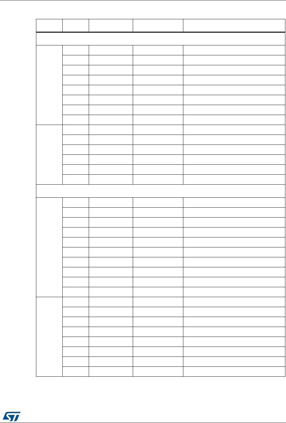
Table 12. Arduino connectors on NUCLEO-F302R8
CN No. Pin No. Pin name MCU pin Function
Left connectors
CN6
Power
1NC - -
2 IOREF - 3.3V Ref
3 RESET NRST RESET
4 +3V3 - 3.3V input/output
5 +5V - 5V output
6 GND - Ground
7 GND - Ground
8 VIN - Power input
CN8
Analog
1 A0 PA0 ADC_IN1
2 A1 PA1 ADC_IN2
3 A2 PA4 ADC_IN5
4 A3 PB0 ADC_IN11
5 A4 PC1 or PB9
(1)
1. Please refer to Table 9: Solder bridges for details.
ADC_IN7 (PC1) or I2C1_SDA (PB9)
6 A5 PC0 or PB8
(1)
ADC_IN6 (PC0) or I2C1_SCL (PB8)
Right connectors
CN5
digital
10 D15 PB8 I2C1_SCL
9 D14 PB9 I2C1_SDA
8 AREF - AVDD
7 GND - Ground
6 D13 PB13 SPI2_SCK
5 D12 PB14 SPI2_MISO
4 D11 PB15 TIM15_CH2 or SPI2_MOSI
3 D10 PB6 TIM16_CH1N or SPI2_CS
2D9 PC7 -
1D8 PA9 -
CN9
digital
8D7 PA8 -
7 D6 PB10 TIM2_CH3
6 D5 PB4 TIM16_CH1
5 D4 PB5 -
4 D3 PB3 TIM2_CH2
3D2 PA10 -
2 D1 PA2 USART2_TX
1 D0 PA3 USART2_RX