
User Manual

Hardware UM2042
14/25 DocID029132 Rev 2
2.3 PCB layout
2.3.1 PCB overview
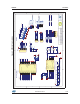
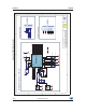
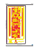
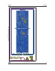
The PCB (see Figure 8) is organized in two halves
• Left side: the SPI header P204 and the digital / MCU sections
• Right side: the analog parts and the ST25R3911B.
The whole PCB is surrounded by a two turns NFC antenna.
Figure 8. PCB overview
The boot button can be found right above the I2C header. If this button is pressed during the
powering or the resetting of the board, the STM32L4 will enter the boot loader mode. The
reset button is positioned between the JTAG/SWD header and the I2C header.
2.3.2 PCB layers
The PCB layout is designed considering that the ST25R3911B is a high power RF
transmitter, hence the decoupling capacitors are located as close as possible to the positive
and negative power supply pins, for example VSP_RF and VSN_RF.
Since the chip is using a differential output driver stage, the antenna matching network is
treated as a differential network. The space between the components is kept as small as
possible and the whole network is routed in a completely symmetrical way.
Via stitching and via shielding is used to maintain a low impedance and prevent short return
current loops. The RF traces are protected by via stitching in combination with guard rings
to create a via wall. This keeps the PCB electromagnetically “quiet”.
A via shield is used to create a vertical copper barrier through the PCB. This helps to reduce
crosstalk and electromagnetic interference in any route carrying an RF signal. The RFI
traces and AAT lanes are routed as close as possible to each other.
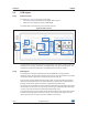
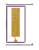
670/
8$57
-7$*6:'
,&
63,
675%
1)&)RUXPPDWFKLQJ
86%
/'29
0DWFKLQJFRPSRQHQWV
069