
Datasheet


1. ELECTRICAL CHARACTERISTICS:
V
DD
= 2.7V
±
0.3V; T
amb
= 0 to 70°C; Rg = 50
Ω
unless otherwise
specified
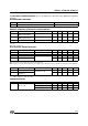
DC OPERATING CONDITIONS
Symbol Parameter Value
V
DD
Power Supply Voltage 2.4 to 3.6V
GENERAL INTERFACE ELECTRICAL CHARACTERISTICS
Symbol Parameter Test Condition Min. Typ. Max. Unit Note
I
IL
Low Level Input Current
Without pull-up device
V
i
= 0V -10 10
µ
A1
I
IH
High Level Input Current
Without pull-up device
V
i
= V
DD
= 3.6V -10 10
µ
A1
V
esd
Electrostatic Protection Leakage < 1
µ
A 2000 V 2
Note 1:
The leakage currents are generally very small, < 1nA. The value given here is a maximum that can occur after an electrostatic stress
on the pin.
Note 2:
Human Body Model.
DC ELECTRICAL CHARACTERISTICS
Symbol Parameter Test Condition Min. Typ. Max. Unit Note
V
IL
Low Level Input Voltage 0.2*V
DD
V
V
IH
High Level Input Voltage 0.8*V
DD
V
V
ol
Low Level Output Voltage I
ol
= Xma 0.4V V 1, 2
V
oh
High Level Output Voltage 0.85*V
DD
V1, 2
Note 1:
Takes into account 200mV voltage drop in both supply lines.
Note 2:
X is the source/sink current under worst case conditions and is reflected in the name of the I/O cell according to the drive capability.
Symbol Parameter Test Condition Min. Typ. Max. Unit Note
I
pu
Pull-up current V
i
= 0V; pin numbers 7, 24
and 26; V
DD
= 3V
-25 -66 -125
µ
A1
R
pu
Equivalent Pull-up
Resistance
50 k
Ω
Note 1:
Min. condition: V
DD
= 2.4V, 125°C Min process
Max. condition: V
DD
= 3.6V, -20°C Max.
POWER DISSIPATION
Symbol Parameter Test Condition Min. Typ. Max. Unit Note
PD Power Dissipation
@ V
DD
= 3V
Sampling_freq
≤
24 kHz 76 mW
Sampling_freq
≤
32 kHz 79 mW
Sampling_freq
≤
48 kHz 85 mW
STA013 - STA013B - STA013T
5/38