
Datasheet


V
DD
100nF
1
2
V
DD
100nF
14
13
V
SS
V
DD
100nF
16
15
V
DD
100nF
23
22
V
SS
V
SS
V
SS
17 18
27
28
26
RESET
24
TESTEN
25
SCANEN
OUT_CLK/DATA_REQ
V
DD
PV
SS
PV
DD
100nF
4.7µF 4.7µF
PV
DD
PV
SS
V
SS
10K
1K
4.7nF
PV
SS
470pF
19
20
21
8
7
6
5
12
11
10
9
4
3
XTO
XTI
SCR_INT
BIT_EN
SCKR
SDI
OCLK
LRCKT
SCKT
SDO
SCL
SDA
D98AU966
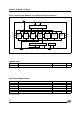
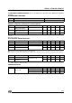
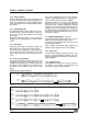
Figure 3.
Test Circuit
I
OL
I
OH
C
L
V
REF
V
DD
OUTPUT
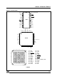
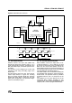
D98AU967
Figure 4.
Test Load Circuit
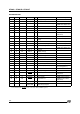
Output I
OL
I
OH
C
L
V
REF
SDA 1mA 100pF 3.6V
Other Outputs 100
µ
A 100
µ
A 100pF 1.5V
Test Load
2. FUNCTIONAL DESCRIPTION
2.1 - Clock Signal
The STA013 input clock is derivated from an ex-
ternal source or from a industry standard crystal
oscillator, generating input frequencies of 10,
14.31818 or 14.7456 MHz.
Other frequencies may be supported upon re-
quest to STMicroelectronics. Each frequency is
supported by downloading a specific configura-
tion file, provided by STM
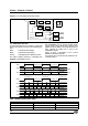
XTI is an input Pad with specific levels.
Symbol Parameter Test Condition Min. Typ. Max. Unit
V
IL
Low Level Input Voltage V
DD
-1.8 V
V
IH
High Level Input Voltage V
DD
-0.8 V
CMOS compatibility
The XTI pad low and high levels are CMOS compatible; XTI pad noise margin is better than typical
CMOS pads.
TTL compatibility
The XTI pad low level is compatible with TTL while the high level is not compatible (for example if V
DD
=
3V TTL min high level = 2.0V while XTI min high level = 2.2V)
STA013 - STA013B - STA013T
6/38