
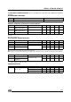
Datasheet
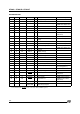

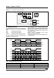
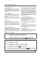

SCLK_POL=0
SCLK_POL=4
DATA IGNOREDDATA VALID
SCKR
SCKR
SDI
BIT_EN
D98AU968A
DATA IGNORED
Figure 6.
Serial Input Interface Clocks
DATA
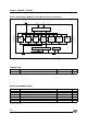
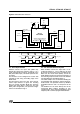
SOURCE
µP
MPEG
DECODER
IIC
D98AU912
IIC
SDO
SCKT
LRCKT
SERIAL AUDIO INTERFACE
SDI
SCKR
BIT_EN
XTO
DAC
RX TX
XTI FILT
PLL
OCLK
SCL SDA
DATA_REQ
Figure 5.
MPEG Decoder Interfaces.
2.2 - Serial Input Interface
STA013 receives the input data (MSB first)
thought the Serial Input Interface (Fig.5). It is a
serial communication interface connected to the
SDI (Serial Data Input) and SCKR (Receiver Se-
rial Clock).
The interface can be configured to receive data
sampled on both rising and falling edge of the
SCKR clock.
The BIT_EN pin, when set to low, forces the bit-
stream input interface to ignore the incoming
data. For proper operation Bit-E
N
line shold be
toggled only when SCR is stable low (for both
SCLK_POL configuration) The possible configu-
rations are described in Fig. 6.
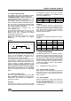
2.3 - PLL & Clock Generator System
When STA013 receives the input clock, as de-
scribed in Section 2.1, and a valid layer III input
bit stream, the internal PLL locks, providing to the
DSP Core the master clock (DCLK), and to the
Audio Output Interface the nominal frequencies of
the incoming compressed bit stream. The STA013
PLL block diagram is described in Figure 7.
The audio sample rates are obtained dividing the
oversampling clock (OCLK) by software program-
mable factors. The operation is done by STA013
embedded software and it is transparent to the
user.
The STA013 PLL can drive directly most of the
commercial DACs families, providing an over
sampling clock, OCLK, obtained dividing the VCO
frequency with a software programmable dividers.
STA013 - STA013B - STA013T
7/38