
Datasheet


Electrical characteristics STCC2540
10/33 DocID024711 Rev 5
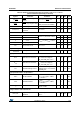
Charger emulator - divider mode
V
DM
DM_IN output voltage
Device set to DCP auto-detect
mode or divider mode,
V
IN
= 5.0 V
1.96 2 2.04 V
V
DP
DP_IN output voltage 2.65 2.7 2.75 V
R
DM
DM_IN output resistance
Device set to DCP auto-detect
mode or divider mode
27 k
R
DP
DP_IN output resistance 27 k
Charger emulator - BC1.2 CDP mode
V
DM_SRC
Voltage source on DM_IN for
CDP detection
V
DP_IN
= 0.6 V, device in CDP
BC1.2 mode
0.5 0.6 0.7 V
V
DAT_REF
DP_IN rising voltage
threshold to turn on
V
DM_SRC
I
DM_IN
= -250 µA, device in
CDP BC1.2 mode
0.25 0.32 0.4 V
V
DAT_REF_HYST
V
DAT_REF
hysteresis 30 mV
V
LGC_SRC
DP_IN rising voltage
threshold to turn off
V
DM_SRC
0.8 1 V
V
LGC_SRC_HYST
V
LGC_SRC
hysteresis 30 mV
I
DP_SINK
DP_IN sink current
0.4 < V
DP_IN
< 0.8 V, device in
CDP BC1.2 mode
50 75 150 µA
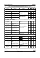
Charger emulator - timings
t
CHG_DGL_ON
Charging indication ON
deglitch delay
From I
OUT
> I
OUT _TH
to
CHARGING
asserted
0.5 s
t
CHG_DGL_OFF
Charging indication OFF
deglitch delay
From I
OUT
<
I
OUT_TH
to
CHARGING
deasserted
5s
t
VDM_SRC_ON
DM_IN voltage source turn-
on time
From V
DP_IN
0 V -> 0.6 V to
V
DM_IN
= V
DM_SRC
, CTLx
configured for CDP BC1.2
8ms
t
VDM_SRC_OFF
DM_IN voltage source turn-
off time
From V
DP_IN
0.6 V -> 0 V to
V
DM_IN
= 0 V, CTLx configured
for CDP BC1.2
1.3 ms
t
VBUS_REAPP
OUT discharge pulse width
From V
OUT
falls to 0.7 V during
discharge to V
OUT
returning to
90%.
300 350 400 ms
Table 4. Electrical characteristics V
IN
= 4.5 to 5.5 V, -40 °C < T
J
< 125 °C
(unless otherwise specified) (continued)
Symbol Parameter Conditions Min. Typ. Max. Unit