
Datasheet
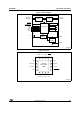


Pin description STCC2540
6/33 DocID024711 Rev 5
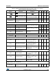
2 Pin description
Table 1. Pin description
Pin no. Name Type Description
1 IN PWR Device and USB port power supply input
2, 3 DM_OUT, DP_OUT I/O USB 2.0 data connection to system USB transmitter (DM = D-, DP = D+)
4 NC - No connect
5ENI
Logic level control input. When EN is low, power switch, data switch and
emulator are OFF.
6, 7, 8 CTL1, CTL2, CTL3 I Logic level control inputs to select charger mode (see Table 5 on page 13).
9 CHARGING O Active low open drain output, asserted when charging current is detected.
10, 11 DP_IN, DM_IN I/O USB 2.0 data connection to system USB connector (DM = D-, DP = D+)
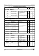
12 OUT PWR USB port power supply output (V
BUS
)
13 FAULT O
Active low open drain output, asserted when overcurrent, overtemperature
or reverse voltage are detected.
14 GND - Ground
15 NC - No connect
16 I
LIM
I Current limit threshold programming resistor terminal.