
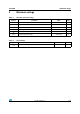
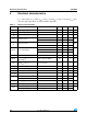
Datasheet

STLD40D Functional description
Doc ID 12203 Rev 7 7/16
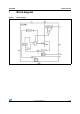
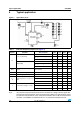
5 Functional description
5.1 Boost controller
The STLD40D is a boost converter operating in PFM (pulsed frequency modulation) mode.
The converter monitors the LED current through the resistor R
LED
and when the feedback
voltage falls below the reference voltage REF2, the boost switch T
SW
turns ON and the
current ramps up. The inductor current is measured by sensing the temperature
compensated drain voltage of the boost MOSFET. The boost turns off when its drain voltage
reaches the internally reference REF1, the main switch remains off until the minimum off
time (250 ns typical) has passed and the feedback voltage is below the reference again. A
maximum ON time of 4 µs typical prevents the switch T
SW
to stay ON during a too long
period of time.
5.2 Adjustable peak inductor current limit
The peak inductor current is monitored by sensing the drain voltage of the switch T
SW
. Since
it exceeds the temperature compensated and supply voltage compensated reference REF1,
the RS flip flop is reset and T
SW
is turned OFF. By connecting a resistance to the pin R
SET
the peak current limit can be adjusted from 200 mA to 1 A. When R
SET
resistor value is
about 12 k
Ω is connected directly to GND, the default value is 1 A.
5.3 Enable
The ENABLE pin is a high logic input signal and allows turning on/off the controller without
cutting the input voltage from the boost regulator circuit. The pin ENABLE can be used to
dim the LED by applying a low frequency PWM signal.
5.4 OVP
If the regulation loop is cut, there is no signal at the feedback pin, the PFM controller will then
continue to switch without control and generate an output voltage at the SW, and V
O
pin
exceeding the breakdown value V
BSW
, and V
BO
.
The over voltage protection (OVP) senses the voltage at the V
O
pin. When the voltage
exceed 38 V min. the controller is automatically turned OFF.
A hysteresis control allows the device restarting automatically since the output voltage drops
down of 1.5 V.