
Datasheet


STM32F050xx Electrical characteristics
Doc ID 023683 Rev 1 39/97
6.3 Operating conditions
6.3.1 General operating conditions
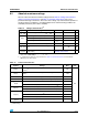
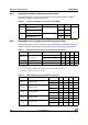
Table 15. General operating conditions
Symbol Parameter Conditions Min Max Unit
f
HCLK
Internal AHB clock frequency 0 48
MHz
f
PCLK
Internal APB clock frequency 0 48
V
DD
Standard operating voltage 2 3.6 V
V
DDA
(1)
Analog operating voltage
(ADC not used)
Must have a potential equal to or
higher than V
DD
23.6
V
Analog operating voltage
(ADC used)
2.4 3.6
V
BAT
Backup operating voltage 1.65 3.6 V
V
IN
I/O input voltage
TC I/O –0.3 V
DD
+0.3
V
TTa I/O –0.3 V
DDA
+0.3
FT and FTf I/O
(2)
–0.3 5.5
BOOT0 0 5.5
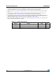
P
D
Power dissipation at T
A
= 85 °C
for suffix 6 or T
A
= 105 °C for
suffix 7
(3)
LQFP48 - 364
mW
UFQFPN32 - 526
UFQFPN28 - 169
TSSOP20 - 182
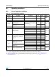
T
A
Ambient temperature for 6
suffix version
Maximum power dissipation –40 85
°C
Low power dissipation
(4)
–40 105
Ambient temperature for 7
suffix version
Maximum power dissipation –40 105
°C
Low power dissipation
(4)
–40 125
T
J Junction temperature range
6 suffix version –40 105
°C
7 suffix version –40 125
1. When the ADC is used, refer to Table 49: ADC characteristics.
2. To sustain a voltage higher than V
DD
+0.3 V, the internal pull-up/pull-down resistors must be disabled.
3. If T
A
is lower, higher P
D
values are allowed as long as T
J
does not exceed T
Jmax
(see Table 14: Thermal characteristics).
4. In low power dissipation state, T
A
can be extended to this range as long as T
J
does not exceed T
Jmax
(see Table 14:
Thermal characteristics).