
Datasheet


Electrical characteristics STM32F050xx
44/97 Doc ID 023683 Rev 1
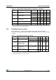
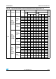
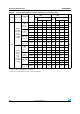
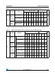
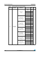
Table 21. Typical and maximum current consumption from the V
DDA
supply
Symbol Parameter
Conditions
(1)
f
HCLK
V
DDA
=
2.4 V V
DDA
=
3.6 V
Unit
Typ
Max @ T
A
(2)
Typ
Max @ T
A
(2)
25 °C 85 °C 105 °C 25 °C 85 °C 105 °C
I
DDA
Supply
current in
Run mode,
code
executing
from Flash
or RAM
HSE
bypass,
PLL on
48 MHz 150 170 178 182 164 183 195 198
µA
32 MHz 104 121 126 128 113 129 135 138
24 MHz 82 96 100 103 88 102 106 108
HSE
bypass,
PLL off
8 MHz 2.0 2.7 3.1 3.3 3.5 3.8 4.1 4.4
1 MHz 2.0 2.7 3.1 3.3 3.5 3.8 4.1 4.4
HSI clock,
PLL on
48 MHz 220 240 248 252 244 263 275 278
32 MHz 174 191 196 198 193 209 215 218
24 MHz 152 167 173 174 168 183 190 192
HSI clock,
PLL off
8 MHz 72 79 82 83 83.5 91 94 95
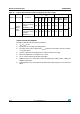
Supply
current in
Sleep
mode,
code
executing
from Flash
or RAM
HSE
bypass,
PLL on
48 MHz 150 170 178 182 164 183 195 198
32 MHz 104 121 126 128 113 129 135 138
24 MHz 82 96 100 103 88 102 106 108
HSE
bypass,
PLL off
8 MHz 2.0 2.7 3.1 3.3 3.5 3.8 4.1 4.4
1 MHz 2.0 2.7 3.1 3.3 3.5 3.8 4.1 4.4
HSI clock,
PLL on
48 MHz 220 240 248 252 244 263 275 278
32 MHz 174 191 196 198 193 209 215 218
24 MHz 152 167 173 174 168 183 190 192
HSI clock,
PLL off
8 MHz 72 79 82 83 83.5 91 94 95
1. Current consumption from the V
DDA
supply is independent of whether the peripherals are on or off. Furthermore when the
PLL is off, I
DDA
is independent from the frequency.
2. Data based on characterization results, not tested in production.