
Datasheet


STM32F050xx Electrical characteristics
Doc ID 023683 Rev 1 65/97
6.3.13 I/O port characteristics
General input/output characteristics
Unless otherwise specified, the parameters given in Ta bl e 4 5 are derived from tests
performed under the conditions summarized in Table 15: General operating conditions. All
I/Os are CMOS and TTL compliant.
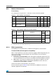
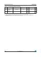
Table 45. I/O static characteristics
Symbol Parameter Conditions Min Typ
Max Unit
V
IL
Low level input
voltage
TC and TTa I/O - - 0.3 V
DD
+0.07
(1)
V
FT and FTf I/O - - 0.475 V
DD
–0.2
(1)
BOOT0 - - 0.3 V
DD
–0.3
(1)
All I/Os except BOOT0 pin - - 0.3 V
DD
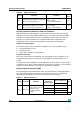
V
IH
High level input
voltage
TC and TTa I/O 0.445 V
DD
+0.398
(1)
--
V
FT and FTf I/O 0.5 V
DD
+0.2
(1)
--
BOOT0 0.2 V
DD
+0.95
(1)
--
All I/Os except BOOT0 pin 0.7 V
DD
--
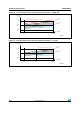
V
hys
Schmitt trigger
hysteresis
TC and TTa I/O - 200
(1)
-
mVFT and FTf I/O - 100
(1)
-
BOOT0 - 300
(1)
-
I
lkg
Input leakage
current
(2)
V
SS
≤V
IN
≤V
DD
I/O TC, FT and FTf
--±0 . 1
µA
V
SS
≤V
IN
≤V
DD
2 V≤V
DD
≤V
DDA
≤3.6 V
I/O TTa used in digital
mode
--±0 . 1
V
IN
= 5 V
I/O FT and FTf
--10
V
IN
= 3.6 V,
2 V≤V
DD
≤V
IN
V
DDA =
3.6 V
I/O TTa used in digital
mode
--1
V
SS
≤V
IN
≤V
DDA
2 V≤V
DD
≤V
DDA
≤3.6 V
I/O TTa used in analog
mode
--±0 . 2
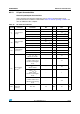
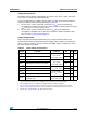
R
PU
Weak pull-up
equivalent
resistor
(3)
V
IN
= V
SS
25 40 55 kΩ