
Datasheet

STM32F051x Electrical characteristics
Doc ID 022265 Rev 3 79/105
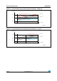
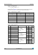
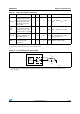
Figure 22. ADC accuracy characteristics
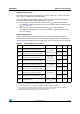
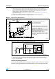
Figure 23. Typical connection diagram using the ADC
1. Refer to Ta bl e 5 4 for the values of R
AIN
, R
ADC
and C
ADC
.
2. C
parasitic
represents the capacitance of the PCB (dependent on soldering and PCB layout quality) plus the
pad capacitance (roughly 7 pF). A high C
parasitic
value will downgrade conversion accuracy. To remedy
this, f
ADC
should be reduced.
General PCB design guidelines
Power supply decoupling should be performed as shown in Figure 10. The 10 nF capacitor
should be ceramic (good quality) and it should be placed as close as possible to the chip.
2. ADC Accuracy vs. Negative Injection Current: Injecting negative current on any of the standard (non-
robust) analog input pins should be avoided as this significantly reduces the accuracy of the conversion
being performed on another analog input. It is recommended to add a Schottky diode (pin to ground) to
standard analog pins which may potentially inject negative current.
Any positive injection current within the limits specified for I
INJ(PIN)
and ΣI
INJ(PIN)
in Section 6.3.13 does not
affect the ADC accuracy.
3. Better performance may be achieved in restricted V
DDA
, frequency and temperature ranges.
4. Data based on characterization results, not tested in production.
E
O
E
G
1LSB
IDEAL
(1) Example of an actual transfer curve
(2) The ideal transfer curve
(3) End point correlation line
E
T
=Total Unadjusted Error: maximum deviation
between the actual and the ideal transfer curves.
E
O
=Offset Error: deviation between the first actual
transition and the first ideal one.
E
G
=Gain Error: deviation between the last ideal
transition and the last actual one.
E
D
=Differential Linearity Error: maximum deviation
between actual steps and the ideal one.
E
L
=Integral Linearity Error: maximum deviation
between any actual transition and the end point
correlation line.
4095
4094
4093
5
4
3
2
1
0
7
6
1234567
4093 4094 4095 4096
(1)
(2)
E
T
E
D
E
L
(3)
V
DDA
V
SSA
-36
1LSB
IDEAL
V
DDA
-36
6
$$!
AINx
I
L
±1 μA
0.6 V
V
T
R
AIN
(1)
C
parasitic
V
AIN
0.6 V
V
T
R
ADC
(1)
12-bit
converter
C
ADC
(1)
Sample and hold ADC
converter