
Datasheet

STM32F051x Package characteristics
Doc ID 022265 Rev 3 99/105
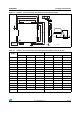
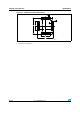
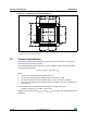
Figure 37. UFQFPN32 - 32-lead ultra thin fine pitch quad flat no-lead package outline (5 x 5)
1. Drawing is not to scale.
2. All leads/pads should also be soldered to the PCB to improve the lead/pad solder joint life.
3. There is an exposed die pad on the underside of the UFQFPN package. This pad is used for the device ground and must
be connected. It is referred to as pin 0 in Table 13: Pin definitions.
Seating plane
ddd C
C
A3
A1
A
D
e
9
16
17
24
32
Pin # 1 ID
R = 0.30
8
E
L
L
D2
1
b
E2
A0B8_ME
Bottom view
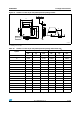
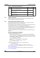
Table 71. UFQFPN32 - 32-lead ultra thin fine pitch quad flat no-lead package (5 x 5),
package mechanical data
Dim.
mm inches
(1)
Min Typ Max Min Typ Max
A 0.5 0.55 0.6 0.0197 0.0217 0.0236
A1 0.00 0.02 0.05 0 0.0008 0.0020
A3 0.152 0.006
b 0.18 0.23 0.28 0.0071 0.0091 0.0110
D 4.90 5.00 5.10 0.1929 0.1969 0.2008
D2 3.50 0.1378
E 4.90 5.00 5.10 0.1929 0.1969 0.2008
E2 3.40 3.50 3.60 0.1339 0.1378 0.1417
e 0.500 0.0197
L 0.30 0.40 0.50 0.0118 0.0157 0.0197
ddd 0.08 0.0031
1. Values in inches are converted from mm and rounded to 4 decimal digits.