
Datasheet
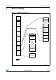
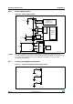

Pinouts and pin description STM32F051x
32/105 Doc ID 022265 Rev 3
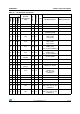
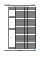
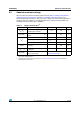
57 41 28 28 PB5 I/O FT
SPI1_MOSI/I2S1_SD,
I2C1_SMBA, TIM16_BKIN,
TIM3_CH2
58 42 29 29 PB6 I/O FTf
I2C1_SCL, USART1_TX,
TIM16_CH1N,
TSC_G5_IO3
59 43 30 30 PB7 I/O FTf
I2C1_SDA, USART1_RX,
TIM17_CH1N,
TSC_G5_IO4
60 44 31 31 BOOT0 I B Boot memory selection
61 45 - 32 PB8 I/O FTf
(3)
I2C1_SCL, CEC,
TIM16_CH1, TSC_SYNC
62 46 - - PB9 I/O FTf
I2C1_SDA, IR_OUT,
TIM17_CH1, EVENTOUT
63 47 32 0 VSS S Ground
64 48 1 1 VDD S Digital power supply
1. PC13, PC14 and PC15 are supplied through the power switch. Since the switch only sinks a limited amount of current
(3 mA), the use of GPIO PC13 to PC15 in output mode is limited:
- The speed should not exceed 2 MHz with a maximum load of 30 pF
- these GPIOs must not be used as a current sources (e.g. to drive an LED).
2. After the first backup domain power-up, PC13, PC14 and PC15 operate as GPIOs. Their function then depends on the
content of the Backup registers which is not reset by the main reset. For details on how to manage these GPIOs, refer to
the Battery backup domain and BKP register description sections in the reference manual.
3. On LQFP32 package, PB2 and PB8 should be treated as unconnected pins (even when they are not available on the
package, they are not forced to a defined level by hardware).
4. After reset, these pins are configured as SWDAT and SWCLK alternate functions, and the internal pull-up on SWDAT pin
and internal pull-down on SWCLK pin are activated.
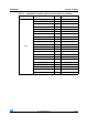
Table 13. Pin definitions (continued)
Pin number
Pin name
(function after
reset)
Pin type
I/O structure
Notes
Pin functions
LQFP64
LQFP48
LQFP32
UFQFPN32
Alternate functions Additional functions