
Datasheet

Electrical characteristics STM32F051x
42/105 Doc ID 022265 Rev 3
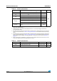
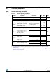
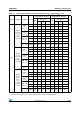
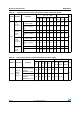
Table 18. Current characteristics
Symbol Ratings Max. Unit
I
VDD
Total current into V
DD
power lines (source)
(1)
1. All main power (V
DD
, V
DDA
) and ground (V
SS
, V
SSA
) pins must always be connected to the external power
supply, in the permitted range.
100
mA
I
VSS
Total current out of V
SS
ground lines (sink)
(1)
100
I
IO
Output current sunk by any I/O and control pin 25
Output current source by any I/Os and control pin − 25
I
INJ(PIN)
Injected current on FT, FTf and B pins -5
(2)
2. Positive injection is not possible on these I/Os and does not occur for input voltages lower than the
specified maximum value.
Injected current on TC and RST pin ± 5
(3)
3. A positive injection is induced by V
IN
>V
DD
while a negative injection is induced by V
IN
<V
SS
. I
INJ(PIN)
must
never be exceeded. Refer also to Table 17: Voltage characteristics for the maximum allowed input voltage
values.
Injected current on TTa pins ± 5
(4)
4. A positive injection is induced by V
IN
>V
DDA
while a negative injection is induced by V
IN
<V
SS
. I
INJ(PIN)
must
never be exceeded. Refer also to Table 17: Voltage characteristics for the maximum allowed input voltage
values. Negative injection disturbs the analog performance of the device. See note 2 below Table 56 on
page 78.
ΣI
INJ(PIN)
Total injected current (sum of all I/O and control
pins)
(5)
5. When several inputs are submitted to a current injection, the maximum ΣI
INJ(PIN)
is the absolute sum of the
positive and negative injected currents (instantaneous values).
± 25
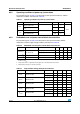
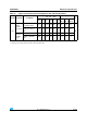
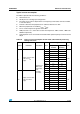
Table 19. Thermal characteristics
Symbol Ratings Value Unit
T
STG
Storage temperature range –65 to +150 °C
T
J
Maximum junction temperature 150 °C