
Datasheet

Electrical characteristics STM32F051x
70/105 Doc ID 022265 Rev 3
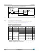
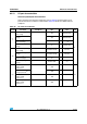
All I/Os are CMOS and TTL compliant (no software configuration required). Their
characteristics cover more than the strict CMOS-technology or TTL parameters. The
coverage of these requirements is shown in Figure 16 and Figure 17 for standard I/Os, and
in Figure 18 and Figure 19 for 5 V tolerant I/Os.
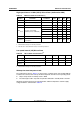
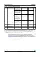
I
lkg
Input leakage current
(3)
V
SS
≤ V
IN
≤ V
DD
I/O TC, FT and FTf
--±0.1
µA
V
SS
≤ V
IN
≤ V
DD
2 V≤ V
DD
≤ V
DDA
≤ 3.6 V
I/O TTa used in digital
mode
--±0.1
V
IN
= 5 V
I/O FT and FTf
--10
V
IN
= 3.6 V,
2 V≤ V
DD
≤ V
IN
V
DDA =
3.6 V
I/O TTa used in digital
mode
--1
V
SS
≤ V
IN
≤ V
DDA
2 V≤ V
DD
≤ V
DDA
≤ 3.6 V
I/O TTa used in analog
mode
--±0.2
R
PU
Weak pull-up equivalent
resistor
(4)
V
IN
= V
SS
30 40 50 kΩ
R
PD
Weak pull-down
equivalent resistor
(4)
V
IN
= V
DD
30 40 50 kΩ
C
IO
I/O pin capacitance - 5 - pF
1. To sustain a voltage higher than V
DD
+0.3 the internal pull-up/pull-down resistors must be disabled.
2. Hysteresis voltage between Schmitt trigger switching levels. Data based on characterization, not tested in production.
3. Leakage could be higher than max. if negative current is injected on adjacent pins.
4. Pull-up and pull-down resistors are designed with a true resistance in series with a switchable PMOS/NMOS. This
MOS/NMOS contribution
to the series resistance is minimum (~10% order).
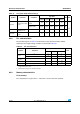
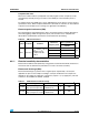
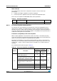
Table 50. I/O static characteristics (continued)
Symbol Parameter Conditions Min Typ
Max Unit