STM6510 Dual push-button Smart ResetTM with capacitor-adjustable delays Features ■ Dual Smart Reset™ push-button inputs with capacitor-adjustable extended reset setup delay (tSRC) ■ Capacitor-adjustable reset pulse duration (tREC) ■ Power-on reset – RST active-low, open-drain ■ Factory-programmable thresholds to monitor VCC in the range of 1.575 to 4.625 V typ. ■ Operating voltage 1.0 V (active-low output valid) to 5.5 V ■ Low supply current (1.
Contents STM6510 Contents 1 Description . . . . . . . . . . . . . . . . . . . . . . . . . . . . . . . . . . . . . . . . . . . . . . . . . 5 1.1 Smart Reset™ devices . . . . . . . . . . . . . . . . . . . . . . . . . . . . . . . . . . . . . . . 5 1.2 STM6510 . . . . . . . . . . . . . . . . . . . . . . . . . . . . . . . . . . . . . . . . . . . . . . . . . . 5 1.3 Pin descriptions . . . . . . . . . . . . . . . . . . . . . . . . . . . . . . . . . . . . . . . . . . . . . 9 1.3.1 Power supply (VCC) . . .
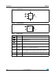
STM6510 List of tables List of tables Table 1. Table 2. Table 3. Table 4. Table 5. Table 6. Table 7. Table 8. Table 9. Table 10. Table 11. Table 12. Table 13. Table 14. Signal names . . . . . . . . . . . . . . . . . . . . . . . . . . . . . . . . . . . . . . . . . . . . . . . . . . . . . . . . . . . . 6 tSRC programmed by an ideal external capacitor . . . . . . . . . . . . . . . . . . . . . . . . . . . . . . . . 9 tREC programmed by an ideal external capacitor . . . . . . . . . . . . . . . . . . . . . . .
List of figures STM6510 List of figures Figure 1. Figure 2. Figure 3. Figure 4. Figure 5. Figure 6. Figure 7. Figure 8. Figure 9. Figure 10. Figure 11. Figure 12. Figure 13. Figure 14. Figure 15. Figure 16. Figure 17. Figure 18. 4/26 Logic diagram . . . . . . . . . . . . . . . . . . . . . . . . . . . . . . . . . . . . . . . . . . . . . . . . . . . . . . . . . . . . 6 Pin connections . . . . . . . . . . . . . . . . . . . . . . . . . . . . . . . . . . . . . . . . . . . . . . . . . . . . . . . . . .
STM6510 Description 1 Description 1.1 Smart Reset™ devices The Smart Reset™ device family STM65xx provides a useful feature that ensures inadvertent short reset push-button closures do not cause system resets. This is done by implementing an extended Smart Reset™ input delay (tSRC). Once the valid Smart Reset™ input levels and setup delay are met, the device generates an output reset pulse with userprogrammable timeout period (tREC).
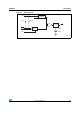
Description STM6510 Figure 1. Logic diagram VCC SR0 RST STM6510 SR1 TRECADJ SRC VSS Figure 2. AM00389a Pin connections RST 1 8 VCC VSS 2 7 SR0 SR1 3 6 TRECADJ NC 4 5 SRC STM 6510 AM00390 Table 1. Symbol Input/output RST Output SR0 Input Primary push-button Smart Reset™ input. Active-low, internal 65 kΩ pull-up resistor to VCC. SR1 Input Secondary push-button Smart Reset™ input. Active-low, internal 65 kΩ pull-up resistor to VCC.
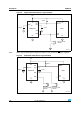
STM6510 Description Figure 3.
Description STM6510 Figure 4. Single-button Smart Reset™ typical hookup VCC 100 kΩ VCC TRECADJ CtREC RESET RST VCC SRC CSRC STM6510 MCU SR1 INT/ NMI SR0 VSS VSS PUSH-BUTTON SWITCH AM04870v1 Note: When only one Smart Reset™ input push-button is used, tie both the SR inputs together. Figure 5.
STM6510 Description 1.3 Pin descriptions 1.3.1 Power supply (VCC) This pin is used to provide the power to the Smart Reset™ device and to monitor the power supply. A 0.1 µF decoupling ceramic capacitor is recommended to be connected between the VCC and VSS pins. 1.3.2 Ground (VSS) This is the supply ground for the device. 1.3.3 Smart Reset™ push-button inputs (SR0, SR1) Both SR0 and SR1 need to be held active at the same time for at least tSRC to activate the reset output pulse.
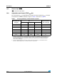
Description 1.3.5 STM6510 Reset output (RST) RST is active-low, open-drain. 1.3.6 Adjustable reset timeout (TRECADJ pin) The reset timeout (tREC) is adjustable by connecting an external capacitor CtREC to this pin. Calculated tREC and CtREC examples are given in Table 3. Refer also to Table 6. Table 3. tREC programmed by an ideal external capacitor Calculated CtREC value [µF] tREC [ms](1)(2) Min. Typ. Max. Closest common CtREC value [µF] 0.001 10 15 20 0.001 0.002 20 30 40 0.0022 0.
STM6510 Typical operating characteristics 2 Typical operating characteristics Figure 7. Supply current (ICC) vs. temperature 2.4 2.2 2 1.8 1.6 ICC [μA] 1.4 1.2 1 0.8 0.6 0.4 0.2 0 -60 -40 -20 0 20 40 60 80 100 120 140 Temperature [°C] 5.5 V Figure 8. 3.3 V 5V 3V AM04876v1 Smart Reset™ delay (tSRC) vs. temperature, CSRC = 0.56 µF 12 11 tSRC [s] 10 9 8 7 6 -60 -40 -20 0 20 40 60 80 100 120 140 Temperature [°C] 5.75 V 5.5 V 3.
Typical operating characteristics Figure 9. STM6510 Reset timeout period (tREC) vs. temperature, CtREC = 0.01 µF 200 190 180 170 tREC [ms] 160 150 140 130 120 110 100 -60 -40 -20 0 20 40 60 80 100 120 140 Temperature [°C] 5.75 V 5.5 V 3.3 V AM04878v1 Figure 10. Reset threshold (VRST) vs. temperature, “S” threshold option, VCC falling 2.99 2.97 VRST [V] 2.95 2.93 2.91 2.89 2.87 2.
STM6510 3 Maximum ratings Maximum ratings Stressing the device above the rating listed in the Table 4: Absolute maximum ratings may cause permanent damage to the device. These are stress ratings only and operation of the device at these or any other conditions above those indicated in the Operating sections of this specification is not implied. Exposure to absolute maximum rating conditions for extended periods may affect device reliability.
DC and AC parameters 4 STM6510 DC and AC parameters This section summarizes the operating measurement conditions, and the DC and AC characteristics of the device. The parameters in the Table 6: DC and AC characteristics that follow, are derived from tests performed under the Measurement Conditions summarized in Table 5: Operating and measurement conditions. Designers should check that the operating conditions in their circuit match the operating conditions when relying on the quoted parameters. Table 5.
STM6510 Table 6. Symbol DC and AC parameters DC and AC characteristics VCC Supply voltage range ICC Supply current (VCC) VOL VRST Test conditions(1) Parameter Reset output voltage low Min. Reset output valid - active-low 1.0 VCC = 5.0 V VCC = 3.0 V 1.5 (3) VCC to reset delay(4) tREC(4) Units 5.5 V 2.4 µA µA VCC ≥ 4.5 V, sinking 3.2 mA 0.3 V VCC ≥ 3.3 V, sinking 2.5 mA 0.3 V VCC ≥ 1.0 V, sinking 0.1 mA 0.3 V –40 to +85 °C VRST –2.5% VRST VRST +2.5% V 25 °C VRST –2.
DC and AC parameters Table 7. STM6510 Possible VCC voltage thresholds VCC voltage threshold VRST 16/26 ±2.5% (–40 °C to +85 °C) ±2.0% (25 °C) Typ. Unit Min. Max. Min. Max. L (falling) 4.625 4.509 4.741 4.533 4.718 V M (falling) 4.375 4.266 4.484 4.288 4.463 V T (falling) 3.075 2.998 3.152 3.014 3.137 V S (falling) 2.925 2.852 2.998 2.867 2.984 V R (falling) 2.625 2.559 2.691 2.573 2.678 V Z (falling) 2.313 2.255 2.371 2.267 2.359 V Y (falling) 2.188 2.
STM6510 5 Package mechanical data Package mechanical data In order to meet environmental requirements, ST offers these devices in different grades of ECOPACK® packages, depending on their level of environmental compliance. ECOPACK® specifications, grade definitions and product status are available at: www.st.com. ECOPACK® is an ST trademark.
Package mechanical data STM6510 Figure 12. TDFN – 8-lead 2 x 2 x 0.75 mm, 0.5 mm pitch package outline D A B PIN 1 INDEX AREA E 0.10 C 2x 0.10 C 2x TOP VIEW 0.10 C C A1 A SEAT ING PLANE SIDE VIEW 0.08 C e b PIN 1 INDEX AREA 1 4 0.10 C A B Pin#1 ID L 5 8 BOTTOM VIEW 8070540_A Table 8. TDFN – 8-lead 2 x 2 x 0.75 mm, 0.5 mm pitch package mechanical data Dimension (mm) Dimension (inches) Symbol Min. Nom. Max. Min. Nom. Max. A 0.70 0.75 0.80 0.028 0.030 0.031 A1 0.00 0.
STM6510 Package mechanical data Figure 13. Landing pattern - TDFN – 8-lead 2 x 2 mm without thermal pad D P E E1 L b Table 9. AM00441 Parameter for landing pattern - TDFN – 8-lead 2 x 2 mm package Dimension (mm) Parameter Description Min. Nom. Max. L Contact length 1.05 — 1.15 b Contact width 0.25 — 0.30 E Max. land pattern Y-direction — 2.75 — E1 Contact gap spacing — 0.65 — D Max. land pattern X-direction — 1.75 — P Contact pitch — 0.
Package mechanical data STM6510 Figure 14. Carrier tape P0 D P2 T E A0 F Top cover tape W B0 Center lines of cavity K0 P1 User direction of feed AM03073v2 Table 10. Carrier tape dimensions Package W D TDFN8 8.00 +0.30 –0.10 1.50 +0.10/ –0.00 20/26 E P0 P2 F 1.75 4.00 2.00 3.50 ±0.10 ±0.10 ±0.10 ±0.05 A0 B0 K0 P1 T 2.30 ±0.05 2.30 ±0.05 1.00 ±0.05 4.00 ±0.10 0.250 ±0.05 Doc ID 16788 Rev 2 Unit Bulk qty.
STM6510 Package mechanical data Figure 15. Reel dimensions T 40 mm min. acces hole at slot location B D C N A Full radius Tape slot in core for tape start 25 mm min width G measured at hub AM00443 Table 11. Reel dimensions Tape sizes A max. B min. C D min. N min. G T max. 8 mm 180 (7 inches) 1.50 13.0 +/– 0.20 20.20 60 8.4 +2/–0 14.
Package mechanical data STM6510 Figure 16. Tape trailer/leader End Top cover tape Start No components Components 100 mm min. T RA IL ER No components L EA D ER 160 mm min. 400 mm min. Sealed with cover tape User direction of feed AM00444 Figure 17. Pin 1 orientation User direction of feed Note: 22/26 1 Drawings are not to scale. 2 All dimensions are in mm, unless otherwise noted.
STM6510 Part numbering 6 Part numbering Table 12. Ordering information scheme Example: STM6510 W C A C DG 6 F Device type STM6510 Reset (VCC monitoring threshold) voltage VRST L = 4.625 V (typ., falling) M = 4.375 V T = 3.075 V S = 2.925 V R = 2.625 V Z = 2.313 V Y = 2.188 V W = 1.665 V V = 1.
Package marking 7 Package marking Table 13. Note: STM6510 Package marking Part name tSRC delay control Smart Reset™ inputs type VRST STM6510WCACDG6F CSRC AL, PU W AL, OD CtREC 8WK STM6510SCACDG6F CSRC AL, PU S AL, OD CtREC 8SK STM6510RCACDG6F CSRC AL, PU R AL, OD CtREC 8RK Reset tREC Topmark output type programming AL = Active-Low, AH = Active-High; PU = with internal pull-up resistor, OD = Open-Drain. Figure 18.
STM6510 8 Revision history Revision history Table 14. Document revision history Date Revision Changes 12-Feb-2010 1 Initial release. 26-Feb-2010 2 Updated title of datasheet, Features, Applications; updated footnote 1 of Table 2; updated Table 6, 12, 13; Figure 3; Section 1.3.3; minor textual and formatting changes.
STM6510 Please Read Carefully: Information in this document is provided solely in connection with ST products. STMicroelectronics NV and its subsidiaries (“ST”) reserve the right to make changes, corrections, modifications or improvements, to this document, and the products and services described herein at any time, without notice. All ST products are sold pursuant to ST’s terms and conditions of sale.