
Datasheet

Electrical characteristics STM8AF52/62xx, STM8AF51/61xx
58/110 Doc ID 14395 Rev 9
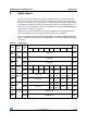
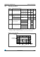
Table 23. Current characteristics
Symbol Ratings Max. Unit
I
VDDIO
Total current into V
DDIO
power lines (source)
(1)(2)(3)
1. All power (V
DD
, V
DDIO
, V
DDA
) and ground (V
SS
, V
SSIO
, V
SSA
) pins must always be connected to the
external supply.
2. The total limit applies to the sum of operation and injected currents.
3. V
DDIO
includes the sum of the positive injection currents. V
SSIO
includes the sum of the negative injection
currents.
100
mA
I
VSSIO
Total current out of V
SS IO
ground lines (sink)
(1)(2)(3)
100
I
IO
Output current sunk by any I/O and control pin 20
Output current source by any I/Os and control pin -20
I
INJ(PIN)
(4)
4. This condition is implicitly insured if VIN maximum is respected. If VIN maximum cannot be respected, the
injection current must be limited externally to the IINJ(PIN) value. A positive injection is induced by VIN >
VDD while a negative injection is induced by VIN < VSS. For true open-drain pads, there is no positive
injection current allowed and the corresponding VIN maximum must always be respected.
Injected current on any pin ±10
I
INJ(TOT)
Sum of injected currents 50
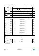
Table 24. Thermal characteristics
Symbol Ratings Value Unit
T
STG
Storage temperature range -65 to 150
°C
T
J
Maximum junction temperature 160
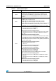
Table 25. Operating lifetime
(1)
1. For detailed mission profile analysis, please contact your local ST Sales Office.
Symbol Ratings Value Unit
OLF Conforming to AEC-Q100 rev G
−40 to 125 °C Grade 1
−40 to 150 °C Grade 0