
Datasheet

STM8AF52/62xx, STM8AF51/61xx Electrical characteristics
Doc ID 14395 Rev 9 71/110
10.3.6 I/O port pin characteristics
General characteristics
Subject to general operating conditions for V
DD
and T
A
unless otherwise specified. All
unused pins must be kept at a fixed voltage, using the output mode of the I/O for example or
an external pull-up or pull-down resistor.
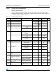
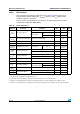
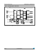
Table 40. I/O static characteristics
Symbol Parameter Conditions Min Typ Max Unit
V
IL
Low-level input voltage
—
-0.3 V 0.3 x V
DD
—
V
IH
High-level input voltage 0.7 x V
DD
V
DD
+ 0.3 V
V
hys
Hysteresis
(1)
—
0.1 x
V
DD
—
V
OH
High-level output voltage
Standard I/0, V
DD
= 5 V,
I = 3 mA
V
DD
- 0.5 V — —
Standard I/0, V
DD
= 3 V,
I = 1.5 mA
V
DD
- 0.4 V — —
V
OL
Low-level output voltage
High sink and true open
drain I/0, V
DD
= 5 V
I = 8 mA
——0.5
VStandard I/0, V
DD
= 5 V
I = 3 mA
——0.6
Standard I/0, V
DD
= 3 V
I = 1.5 mA
——0.4
R
pu
Pull-up resistor V
DD
= 5 V, V
IN
= V
SS
35 50 65 kΩ
t
R
, t
F
Rise and fall time
(10% - 90%)
Fast I/Os
Load = 50 pF
——35
(2)
ns
Standard and high sink I/Os
Load = 50 pF
— — 125
(2)
Fast I/Os
Load = 20 pF
20
(2)
Standard and high sink I/Os
Load = 20 pF
50
(2)
I
lkg
Digital input pad leakage
current
V
SS
≤ V
IN
≤ V
DD
——±1µA
I
lkg ana
Analog input pad leakage
current
V
SS
≤ V
IN
≤ V
DD
-40 °C < T
A
< 125 °C
— — ±250
nA
V
SS
≤ V
IN
≤ V
DD
-40 °C < T
A
< 150 °C
— — ±500
I
lkg(inj)
Leakage current in
adjacent I/O
(3)
Injection current ±4 mA — — ±1
(3)
µA
I
DDIO
Total current on either
V
DDIO
or V
SSIO
Including injection currents — — 60 mA
1. Hysteresis voltage between Schmitt trigger switching levels. Based on characterization results, not tested in production.