
Datasheet
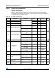

Electrical characteristics STM8AF52/62xx, STM8AF51/61xx
76/110 Doc ID 14395 Rev 9
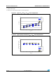
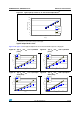
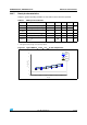
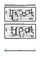
Figure 36. Typical NRST pull-up resistance R
PU
vs V
DD
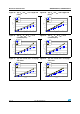
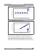
Figure 37. Typical NRST pull-up current I
pu
vs V
DD
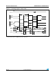
The reset network shown in Figure 38 protects the device against parasitic resets. The user
must ensure that the level on the NRST pin can go below V
IL(NRST)
max (see Table 41:
NRST pin characteristics), otherwise the reset is not taken into account internally.
For power consumption sensitive applications, the external reset capacitor value can be
reduced to limit the charge/discharge current. If NRST signal is used to reset external
circuitry, attention must be taken to the charge/discharge time of the external capacitor to
fulfill the external devices reset timing conditions. Minimum recommended capacity is 10 nF.
30
35
40
45
50
55
60
2.5 3 3.5 4 4.5 5 5.5 6
V
DD
[V]
NRST Pull-Up resistance [k ohm]
-40°C
25°C
85°C
125°C
0
20
40
60
80
100
120
140
0123456
V
DD
[V]
NRST Pull-Up current [µA]
-40°C
25°C
85°C
125°C