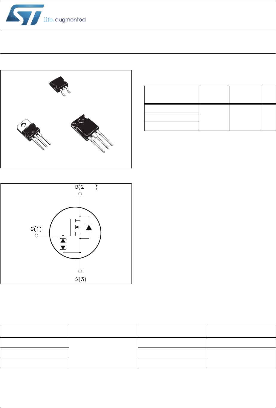
STB18N60M2, STP18N60M2, STW18N60M2 N-channel 600 V, 0.255 Ω typ., 13 A MDmesh II Plus™ low Qg Power MOSFET in D2PAK, TO-220 and TO-247 packages Datasheet - production data Features TAB Order codes 3 1 2 VDS @ TJmax RDS(on) max ID 650 V 0.28 Ω 13 A D PAK STB18N60M2 STP18N60M2 TAB STW18N60M2 • Extremely low gate charge 3 1 3 2 TO-220 2 1 • Lower RDS(on) x area vs previous generation • Low gate input resistance TO-247 • 100% avalanche tested Figure 1.
Contents STB18N60M2, STP18N60M2, STW18N60M2 Contents 1 Electrical ratings . . . . . . . . . . . . . . . . . . . . . . . . . . . . . . . . . . . . . . . . . . . . 3 2 Electrical characteristics . . . . . . . . . . . . . . . . . . . . . . . . . . . . . . . . . . . . . 4 2.1 Electrical characteristics (curves) . . . . . . . . . . . . . . . . . . . . . . . . . . . . . . . . 6 3 Test circuits 4 Package mechanical data . . . . . . . . . . . . . . . . . . . . . . . . . . . . . . . . . . . .
STB18N60M2, STP18N60M2, STW18N60M2 1 Electrical ratings Electrical ratings Table 2. Absolute maximum ratings Symbol Value Unit ± 25 V Gate-source voltage VGS ID Drain current (continuous) at TC = 25 °C 13 A ID Drain current (continuous) at TC = 100 °C 8 A IDM(1) Drain current (pulsed) 52 A PTOT Total dissipation at TC = 25 °C 110 W Peak diode recovery voltage slope 15 V/ns MOSFET dv/dt ruggedness 50 V/ns - 55 to 150 °C dv/dt (2) dv/dt(3) Tstg Storage temperature Tj 1.
Electrical characteristics 2 STB18N60M2, STP18N60M2, STW18N60M2 Electrical characteristics (TC = 25 °C unless otherwise specified) Table 5. On /off states Symbol V(BR)DSS IDSS IGSS Parameter Drain-source breakdown voltage Test conditions ID = 1 mA, VGS = 0 Min. Typ. V 1 μA 100 μA ±10 μA 3 4 V 0.255 0.28 Ω Min. Typ. Max. Unit - 791 - pF - 40 - pF - 5.
STB18N60M2, STP18N60M2, STW18N60M2 Electrical characteristics Table 8. Source drain diode Symbol Parameter Test conditions Min. Typ. Max. Unit Source-drain current - 13 A ISDM (1) Source-drain current (pulsed) - 52 A VSD (2) Forward on voltage - 1.
Electrical characteristics 2.1 STB18N60M2, STP18N60M2, STW18N60M2 Electrical characteristics (curves) Figure 2. Safe operating area for D2PAK and TO-220 Figure 3. Thermal impedance for D2PAK, TO-220 and TO-247 AM15835v1 ID (A) (o n) 10µs DS Op Lim erat ite ion d b in y m this ax are a R is 10 1 100µs 1ms Tj=150°C Tc=25°C 10ms Single pulse 0.1 10 1 0.1 100 VDS(V) Figure 4. Safe operating area for TO-247 AM15836v1 ID (A) Figure 5.
STB18N60M2, STP18N60M2, STW18N60M2 Figure 8. Static drain-source on-resistance AM15840v1 RDS(on) (Ω) Electrical characteristics Figure 9. Capacitance variations AM15841v1 C (pF) VGS=10V 0.270 1000 Ciss 0.265 100 0.260 Coss 0.255 10 0.250 0.245 0 8 6 4 2 10 12 ID(A) Figure 10. Normalized gate threshold voltage vs. temperature AM15828v1 VGS(th) 1 0.1 (norm) Crss 1 100 10 VDS(V) Figure 11. Normalized on-resistance vs temperature AM15829v1 RDS(on) (norm) ID=6.5 A VGS=10V 2.
Electrical characteristics STB18N60M2, STP18N60M2, STW18N60M2 Figure 14.
STB18N60M2, STP18N60M2, STW18N60M2 3 Test circuits Test circuits Figure 15. Switching times test circuit for resistive load Figure 16. Gate charge test circuit VDD 12V 47kΩ 1kΩ 100nF 3.3 μF 2200 RL μF IG=CONST VDD VGS 100Ω Vi=20V=VGMAX VD RG 2200 μF D.U.T. D.U.T. VG 2.7kΩ PW 47kΩ 1kΩ PW AM01468v1 Figure 17. Test circuit for inductive load switching and diode recovery times A A AM01469v1 Figure 18. Unclamped inductive load test circuit L A D G D.U.T.
Package mechanical data 4 STB18N60M2, STP18N60M2, STW18N60M2 Package mechanical data In order to meet environmental requirements, ST offers these devices in different grades of ECOPACK® packages, depending on their level of environmental compliance. ECOPACK® specifications, grade definitions and product status are available at: www.st.com. ECOPACK® is an ST trademark.
STB18N60M2, STP18N60M2, STW18N60M2 Package mechanical data Figure 21.
Package mechanical data STB18N60M2, STP18N60M2, STW18N60M2 Table 9. D²PAK (TO-263) mechanical data mm Dim. Min. Typ. A 4.40 4.60 A1 0.03 0.23 b 0.70 0.93 b2 1.14 1.70 c 0.45 0.60 c2 1.23 1.36 D 8.95 9.35 D1 7.50 E 10 E1 8.50 10.40 e 2.54 e1 4.88 5.28 H 15 15.85 J1 2.49 2.69 L 2.29 2.79 L1 1.27 1.40 L2 1.30 1.75 R V2 12/21 Max. 0.
STB18N60M2, STP18N60M2, STW18N60M2 Package mechanical data Figure 22. D²PAK footprint(a) 16.90 12.20 5.08 1.60 3.50 9.75 Footprint a.
Package mechanical data STB18N60M2, STP18N60M2, STW18N60M2 Figure 23.
STB18N60M2, STP18N60M2, STW18N60M2 Package mechanical data Table 10. TO-220 type A mechanical data mm Dim. Min. Typ. Max. A 4.40 4.60 b 0.61 0.88 b1 1.14 1.70 c 0.48 0.70 D 15.25 15.75 D1 1.27 E 10 10.40 e 2.40 2.70 e1 4.95 5.15 F 1.23 1.32 H1 6.20 6.60 J1 2.40 2.72 L 13 14 L1 3.50 3.93 L20 16.40 L30 28.90 ∅P 3.75 3.85 Q 2.65 2.
Package mechanical data STB18N60M2, STP18N60M2, STW18N60M2 Figure 24.
STB18N60M2, STP18N60M2, STW18N60M2 Package mechanical data Table 11. TO-247 mechanical data mm. Dim. Min. Typ. Max. A 4.85 5.15 A1 2.20 2.60 b 1.0 1.40 b1 2.0 2.40 b2 3.0 3.40 c 0.40 0.80 D 19.85 20.15 E 15.45 15.75 e 5.30 L 14.20 14.80 L1 3.70 4.30 5.45 L2 5.60 18.50 ∅P 3.55 3.65 ∅R 4.50 5.50 S 5.30 5.50 DocID024735 Rev 2 5.
Packaging mechanical data 5 STB18N60M2, STP18N60M2, STW18N60M2 Packaging mechanical data Figure 25. Tape 10 pitches cumulative tolerance on tape +/- 0.2 mm T P0 Top cover tape P2 D E F B1 K0 For machine ref.
STB18N60M2, STP18N60M2, STW18N60M2 Packaging mechanical data Figure 26. Reel T REEL DIMENSIONS 40mm min. Access hole At slot location B D C N A Full radius G measured at hub Tape slot in core for tape start 25 mm min. width AM08851v2 Table 12. D²PAK (TO-263) tape and reel mechanical data Tape Reel mm mm Dim. Dim. Min. Max. A0 10.5 10.7 A B0 15.7 15.9 B 1.5 D 1.5 1.6 C 12.8 D1 1.59 1.61 D 20.2 E 1.65 1.85 G 24.4 F 11.4 11.6 N 100 K0 4.8 5.0 T P0 3.9 4.
Revision history 6 STB18N60M2, STP18N60M2, STW18N60M2 Revision history Table 13. Document revision history 20/21 Date Revision Changes 05-Jun-2013 1 First release.
STB18N60M2, STP18N60M2, STW18N60M2 Please Read Carefully: Information in this document is provided solely in connection with ST products. STMicroelectronics NV and its subsidiaries (“ST”) reserve the right to make changes, corrections, modifications or improvements, to this document, and the products and services described herein at any time, without notice. All ST products are sold pursuant to ST’s terms and conditions of sale.