
Datasheet


Table Of Contents
- Figure 1. Internal schematic diagram
- Table 1. Device summary
- 1 Electrical ratings
- 2 Electrical characteristics
- Table 5. On /off states
- Table 6. Dynamic
- Table 7. Switching times
- Table 8. Source drain diode
- 2.1 Electrical characteristics (curves)
- Figure 2. Safe operating area for D2PAK and TO-220
- Figure 3. Thermal impedance for D2PAK, TO-220 and TO-247
- Figure 4. Safe operating area for TO-247
- Figure 5. Output characteristics
- Figure 6. Transfer characteristics
- Figure 7. Gate charge vs gate-source voltage
- Figure 8. Static drain-source on-resistance
- Figure 9. Capacitance variations
- Figure 10. Normalized gate threshold voltage vs. temperature
- Figure 11. Normalized on-resistance vs temperature
- Figure 12. Source-drain diode forward characteristics
- Figure 13. Normalized V(BR)DSS vs temperature
- Figure 14. Output capacitance stored energy
- 3 Test circuits
- 4 Package mechanical data
- 5 Packaging mechanical data
- 6 Revision history
DocID024735 Rev 2 3/21
STB18N60M2, STP18N60M2, STW18N60M2 Electrical ratings
21
1 Electrical ratings
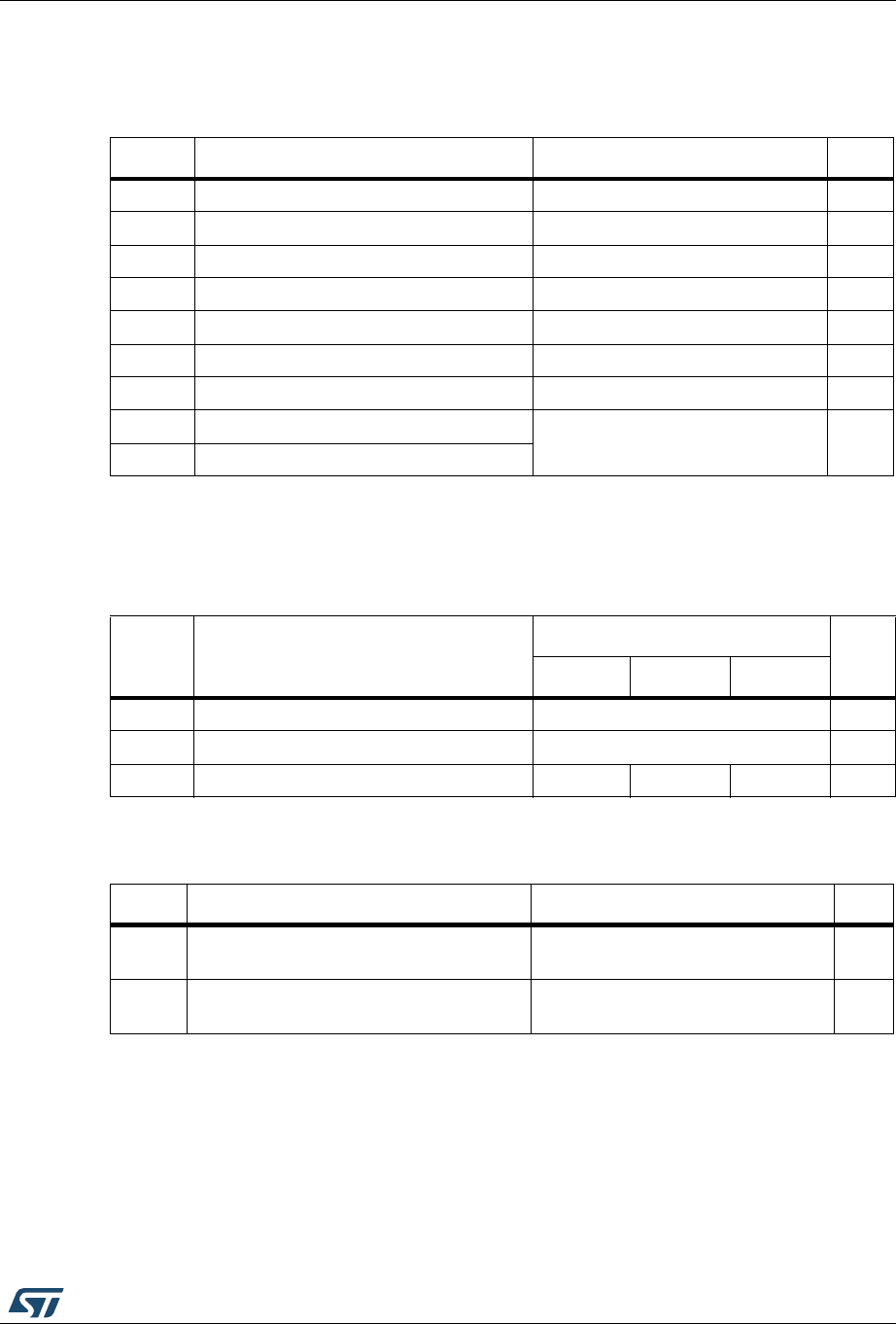
Table 2. Absolute maximum ratings
Symbol Parameter Value Unit
V
GS
Gate-source voltage ± 25 V
I
D
Drain current (continuous) at T
C
= 25 °C 13 A
I
D
Drain current (continuous) at T
C
= 100 °C 8 A
I
DM
(1)
1. Pulse width limited by safe operating area
Drain current (pulsed) 52 A
P
TOT
Total dissipation at T
C
= 25 °C 110 W
dv/dt
(2)
2. I
SD
≤ 13 A, di/dt ≤ 400 A/μs; V
DS
peak
< V
(BR)DSS
, V
DD
=400 V.
Peak diode recovery voltage slope 15 V/ns
dv/dt
(3)
3. V
DS
≤ 480 V
MOSFET dv/dt ruggedness 50 V/ns
T
stg
Storage temperature
- 55 to 150 °C
T
j
Max. operating junction temperature
Table 3. Thermal data
Symbol Parameter
Value
Unit
D
2
PAK TO-220 TO-247
R
thj-case
Thermal resistance junction-case max 1.14 °C/W
R
thj-amb
Thermal resistance junction-ambient max 62.5 °C/W
R
thj-pcb
(1)
1. When mounted on 1 inch² FR-4, 2 Oz copper board
Thermal resistance junction-pcb max 30 °C/W
Table 4. Avalanche characteristics
Symbol Parameter Value Unit
I
AR
Avalanche current, repetitive or not
repetitive (pulse width limited by T
jmax
)
3A
E
AS
Single pulse avalanche energy (starting
T
j
=25°C, I
D
= I
AR
; V
DD
=50)
135 mJ