
Datasheet


TIP140 TIP141 TIP142 TIP145 TIP146 TIP147
http://onsemi.com
4
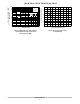
ACTIVE–REGION SAFE OPERATING AREA
There are two limitations on the power handling ability of
a transistor: average junction temperature and second
breakdown. Safe operating area curves indicate I
C
– V
CE
limits of the transistor that must be observed for reliable
operation; i.e., the transistor must not be subjected to greater
dissipation than the curves indicate.
The data of Figure 6 is based on T
J(pk)
= 150C; T
C
is
variable depending on conditions. At high case
temperatures, thermal limitations will reduce the power that
can be handled to values less than the limitations imposed by
second breakdown.
SECONDARY BREAKDOWN LIMIT
BONDING WIRE LIMIT
THERMAL LIMITATION @ T
C
= 25°C
Figure 6. Active–Region Safe Operating Area
dc
V
CE
, COLLECTOR-EMITTER VOLTAGE (VOLTS)
2.0
I
C
, COLLECTOR CURRENT (AMP) (mA)
10
10
0.2
5.0
20
1.0
20
T
J
= 150°C
5030
TIP140, 145
3.0
7.0
15 70 100
TIP141, 146
TIP142, 147
I
C
, COLLECTOR CURRENT (AMPS)
15
10
1.0
2.0
5.0
7.0
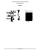
Figure 7. Unclamped Inductive Load
L, UNCLAMPED INDUCTIVE LOAD (mH)
0.5 1.0 2.0 5.0 10 20 50 100
100 mJ
INPUT
MPS-U52
50
50
R
BB1
1.5k
R
BB2
= 100
V
BB2
= 0
V
BB1
= 10 V
TUT
V
CE
MONITOR
100 mH
V
CC
= 20 V
I
C
MONITOR
R
S
= 0.1
TEST CIRCUIT
NOTE 1: Input pulse width is increased until I
CM
= 1.42 A.
NOTE 2: For NPN test circuit reverse polarities.
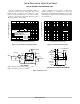
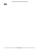
INPUT
VOLTAGE
COLLECTOR
CURRENT
1.42 A
V
CE(sat)
-20 V
COLLECTOR
VOLTAGE
V
(BR)CER
w ≈ 7.0 ms (SEE NOTE 1)
5.0 V
0
100 ms
0
VOLTAGE AND CURRENT WAVEFORMS
Figure 8. Inductive Load