
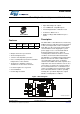
Datasheet


DocID14174 Rev 13 3/25
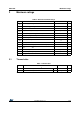
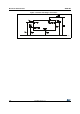
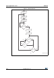
VNI4140K Pin connection
25
1 Pin connection
Figure 2. Pin connection (top view)
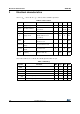
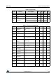
Table 1. Pin description
Pin Name Description
Tab TAB Exposed tab internally connected to V
cc
1V
CC
Supply voltage
2 IN1 Channel 1 input 3.3 V CMOS/TTL compatible
3 STAT1 Channel 1 status in open drain configuration
4 IN2 Channel 2 input 3.3 V CMOS/TTL compatible
5 STA2 Channel 2 status in open drain configuration
6 GND Device ground connection
7 STAT3 Channel 3 status in open drain configuration
8 IN3 Channel 3 input 3.3 V CMOS/TTL compatible
9 STAT4 Channel 4 status in open drain configuration
10 IN4 Channel 4 input 3.3 V CMOS/TTL compatible
11 NC
12 NC
13 OUT4 Channel 4 power stage output, internally protected
14 OUT4 Channel 4 power stage output, internally protected
15 OUT4 Channel 4 power stage output, internally protected
16 OUT3 Channel 3 power stage output, internally protected
17 OUT3 Channel 3 power stage output, internally protected
OUT1
OUT1
OUT1
OUT2
OUT2
OUT2
V
CC
IN1
STAT1
IN2
STAT2
GND
OUT3
OUT3
OUT3
OUT4
OUT4
OUT4
STAT3
IN3
STAT4
NC
NC
IN4