
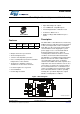
Datasheet

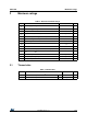

Electrical characteristics VNI4140K
6/25 DocID14174 Rev 13
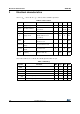
3 Electrical characteristics
10.5 V < V
CC
< 36 V; -40 °C < T
J
< 125 °C; unless otherwise specified
V
CC
= 24 V; -40 °C < T
J
< 125 °C, R
L
= 48 Ω, input rise time < 0.1 µs
Table 4. Power section
Symbol Parameter Test conditions Min. Typ. Max. Unit
V
cc
Supply voltage 10.5 36 V
R
DS(on)
On-state resistance
I
OUT
= 0.5 A at T
J
= 25 °C
I
OUT
= 0.5 A
0.080
0.140
Ω
Ω
V
clamp
I
s
= 20 mA 41 45 52 V
I
S
Supply current
All channels in OFF state
ON state with V
IN
= 5 V
(T
J
= 125 °C)
250
2.4 4
µA
mA
I
LGND
Output current at turn-
off
V
CC
= V
STAT
= V
IN
= V
GND
=
24 V, V
OUT
= 0 V
1mA
V
OUT(OFF)
Off state output
voltage
V
IN
= 0 V and I
OUT
= 0 A 1 V
I
OUT(OFF)
Off state output
current
V
IN
= V
OUT
= 0 V 0 5 µA
F
CP
Charge pump
frequency
Channel in ON state
(1)
1. To cover EN55022 class A and class B normative.
1450 kHz
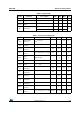
Table 5. Switching
Symbol Parameter Min. Typ. Max. Unit
t
d
(ON)
Turn on delay - 20 - µs
t
r
Rise time - 10 - µs
t
d
(OFF)
Turn off - 30 - µs
t
f
Fall time - 8 - µs
dV/dt
(ON)
Turn on voltage slope - 3 - V/µs
dV/dt
(OFF)
Turn off voltage slope - 4 - V/µs