
Manual

vi
StorCase Technology, Inc. DE100i-A User's Guide - Rev. F01
List of Figures
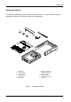
Figure 1: Package Contents .......................................................................................... 1
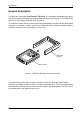
Figure 2: DE100i-A Receiving Frame and Carrier ........................................................ 3
Figure 3: Receiving Frame Front Panel ......................................................................... 4
Figure 4: Receiving Frame Unit ID Number and Activity Display ................................. 4
Figure 5: Receiving Frame Rear Panel ......................................................................... 5
Figure 6: DE100i-A Drive Carrier Circuit Board ............................................................ 7
Figure 7: Typical AT/IDE Drive Connections ............................................................... 10
Figure 8: Drive Installation Assembly .......................................................................... 11
Figure 9: Master/Slave Configuration Jumper J4A .................................................... 12
Figure 10: Receiving Frame Mounting Holes ................................................................ 13
Figure 11: Unit ID Select Switch Location .................................................................... 15
Figure A-1: DE100i-A Physical Dimensions .................................................................... 19
Figure B-1: Attaching the ON/OFF Key .......................................................................... 20
Figure A-1: Carrying Case ............................................................................................... 21
Figure A-2: Full Drive Cover ............................................................................................ 22
Figure A-3: Drive Plug ...................................................................................................... 23
Figure A-4: Solenoid Mechanism .................................................................................... 24
List of Tables
Table 1: J3 Master/Slave Signal Levels ......................................................................... 8
Table 2: J3 Master (No Slave) Signal Levels ................................................................. 9
Table 3: Unit ID Select Switch Settings ........................................................................ 15
Table 4: AT/IDE interface Signals ................................................................................. 16
NOTICE: This User's Guide is subject to periodic updates without notice. While reasonable
efforts have been made to ensure accuracy of this document, StorCase Technol-
ogy, Inc. assumes no liability resulting from errors or omissions in this publication,
or from the use of the information contained herein.
Please check the StorCase web site at http://www.storcase.com or contact your
StorCase representative for the latest revision of this document.