
User's Manual


Summit User’s Guide – SDC-SSD40L
10
SDC-SSD40L_UsersGuide
© 2011 – 2012 Summit Data Communications, Inc. All rights reserved.
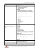
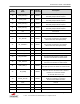
Pin
Number
Pin
Name
I/O
Voltage
Reference
Description
18
SDIO_DATA_2
I/O
VDDIO
SDIO Data 2 – Internal pull-up.
External pull-up resistor required
19
SDIO_CMD
I/O
VDDIO
SDIO Command – Internal pull-up.
External pull-up resistor required
20
SDIO_DATA_3
I/O
VDDIO
SDIO Data 3 – Internal pull-up.
External pull-up resistor required
21
SDIO_DATA_1
I/O
VDDIO
SDIO Data 1 – Internal pull-up.
External pull-up resistor required
22
N/C
N/C
No Connect
23
N/C
N/C
No Connect
24
BT_ACTIVE
I/O
VDDIO
No connect
Not currently supported in the firmware.
When not in use, leave open (float).
25
BT_PRIORITY
I/O
VDDIO
No connect
Not currently supported in the firmware.
When not in use, leave open (float).
26
GND
-
Ground
27
VCC3_3
-
3.3V Module Power
28
VCC3_3
-
3.3V Module Power
29
VIN_IP2LDO-L
O
Unsupported direct battery power output.
Connect to Pin 30 with a 3.3uH inductor.
30
VIN_1P2LDO
I
Unsupported direct battery power input.
Connect to Pin 29 with a 3.3uH inductor.
31
CHIP_PWD_L
I
VDDIO
Powers down the radio, active low;
4.7K pull-up resistor to VDDIO is recommended
32
BT_FREQ
I
VDDIO
Input from BT device.
Indicates that the coexistence BT is about to
transmit on a restricted channel
Tie to GND when not in use
33
WLAN_ACTIVE
O
VDDIO
Output to BT device. When high, indicates that
WLAN is transmitting or receiving.
Do not connect when not used
34
GND
-
Ground
35
GND
-
Ground
36
N/C
N/C
No Connect
37
GND
-
Ground