
Server User Manual
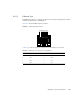
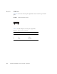
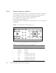
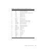
Table Of Contents
- Sun Netra™ CP3250 Blade Server User’s Guide
- Contents
- Figures
- Tables
- Preface
- Overview
- Hardware Installation and Service
- 2.1 Safety and Tool Requirements
- 2.2 Installing the Blade Server
- 2.3 Service Procedures
- 2.3.1 Hot-Swapping the Netra CP3250 Blade Server
- 2.3.2 Powering Off the Netra CP3250 Blade Server
- 2.3.3 Removing the Netra CP3250 Blade Server
- 2.3.4 Powering On the System
- 2.3.5 Automatic Power-Off Events
- 2.3.6 Servicing DIMMs
- 2.3.7 Installing the Optional Compact Flash Card
- 2.3.8 Installing Optional AMC
- 2.3.9 Adding or Replacing the Battery
- 2.3.10 Changing Jumper Settings
- 2.3.11 Checking DIP Switch Settings
- 2.3.12 Resetting the Netra CP3250 Blade Server
- Hardware Architecture
- Software Configuration
- Configuring and Using BIOS Firmware
- 5.1 About BIOS Settings
- 5.2 Changing the Configuration of a BIOS Menu Item
- 5.3 Setting the Boot Device Using BIOS Setup Screens
- 5.4 Setting Supervisor and User Passwords
- 5.5 Resetting the System Time and System Date
- 5.6 Updating the BIOS
- 5.7 Secondary BIOS Image
- 5.8 Perform a Live Firmware Upgrade
- 5.9 Power-On Self-Test
- 5.10 Changing POST Options
- BIOS Screens
- Physical Characteristics
- ShMM CLI and Commands
- Index
B-6 Sun Netra CP3250 Blade Server User’s Guide • April 2009
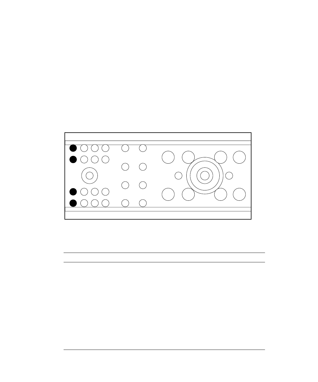
B.3.3 Power Connector (Zone 1)
The Sun Netra CP3250 blade server uses a 34-pin Positronic connector as the Zone 1
power distribution connector. It provides the support for the following signals:
■ Two -48 VDC power feeds (four signals each; eight signals total)
■ Two IPMB ports (two signals each; four signals total)
■ Geographic address (eight signals)
The analog test and ring voltage pins are left unconnected.
FIGURE B-4 shows the pin
assignments.
FIGURE B-4 Power Distribution Connector (Zone 1) P10
TABLE B-4 lists the power distribution connector pin assignments.
TABLE B-4 Power Distribution Connector Pin Assignments
Pin Number Name Description
1 Reserved Reserved
2 Reserved Reserved
3 Reserved Reserved
4 Reserved Reserved
5 HA0 HA0 Hardware Address Bit 0
6 HA1 HA1 Hardware Address Bit 1
7 HA2 HA2 Hardware Address Bit 2
8 HA3 HA3 Hardware Address Bit 3
9 HA4 HA4 Hardware Address Bit 4
113
416
17
20
21
25
26
28
29
27
30
31
33
34
32
24