SME5224AUPA-400 July 1999 UltraSPARC™-II CPU Module 400 MHz CPU, 4.0 MB E-Cache DATASHEET MODULE DESCRIPTION The UltraSPARC™–II, 400 MHz CPU, 4.0 Mbyte module, (SME5224AUPA-400) delivers high performance computing in a compact design. Based on the UltraSPARC™-II CPU, this module is designed using a small form factor board with an integrated external cache. It connects to the high bandwidth Ultra™ Port Architecture UPA bus via a high speed sturdy connector. The UltraSPARC™–II, 400 MHz CPU, 4.
SME5224AUPA-400 UltraSPARC™-II CPU Module 400 MHz CPU, 4.0 MB E-Cache CPU DESCRIPTION UltraSPARC-II CPU The UltraSPARC™-II CPU is the second generation in the UltraSPARC™ s-series microprocessor family. A complete implementation of the SPARC V9 architecture, it has binary compatibility with all previous versions of the SPARC™ microprocessor family. The UltraSPARC™-II CPU is designed as a cost effective, scalable and reliable solution for high-end workstations and servers.
UltraSPARC™-II CPU Module 400 MHz CPU, 4.0 MB E-Cache Advanced Version SME5224AUPA-400 DATA BUFFER DESCRIPTION UltraSPARC-II Data Buffer (UDB-II) The UltraSPARC™-II module has two UltraSPARC-II data buffers (UDB-II) - each a 256 pin BGA device - for a UPA Interconnect system bus width of 128 Data + 16 ECC. There is a bidirectional flow of information between the external cache of the CPU and the 144-bit UPA interconnect.
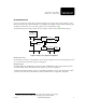
UltraSPARC™-II CPU Module 400 MHz CPU, 4.0 MB E-Cache SME5224AUPA-400 MODULE COMPONENT OVERVIEW The UltraSPARC™–II, 400 MHz CPU, 4.0 Mbyte module, (SME5224AUPA-400), (see Figure 1), consists of the following components: • • • • • • UltraSPARC™-II CPU at 400 MHz UltraSPARC-II Data Buffer (UDB-II) 4.0 Megabyte E-cache, made up of eight (256K X 18) data SRAMs and one 128K X 36 Tag SRAM Clock Buffer: MC100LVE210 DC-DC regulator (2.6V to 1.
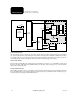
UltraSPARC™-II CPU Module 400 MHz CPU, 4.0 MB E-Cache Advanced Version SME5224AUPA-400 SYSTEM INTERFACE Figure 2 shows the major components of a UPA based uniprocessor system. The system controller [1] for the UPA bus arbitrates between the UltraSPARC™–II, 400 MHz CPU, 4.0 Mbyte module, and the I/O bridge chip. The figure also illustrates a slave-only UPA graphics port for Sun graphics boards . The module UPA system interface signals run at one-quarter of the rate of the internal CPU frequency.
SME5224AUPA-400 UltraSPARC™-II CPU Module 400 MHz CPU, 4.0 MB E-Cache Module ID Module IDs are used to configure the UPA address of a module. The UPA_PORT_ID[4:3] are hardwired on the module to “0”. UPA_PORT_ID[1:0] are brought out to the connector pins. Each module is hardwired in the system to a fixed and unique UPA address. This feature supports systems with four or fewer processors.
UltraSPARC™-II CPU Module 400 MHz CPU, 4.0 MB E-Cache Advanced Version SME5224AUPA-400 SIGNAL DESCRIPTION [1] System Interface Signal Type Name and Function UPA_ADDR[35:0] I/O Packet switched transaction request bus. Maximum of three other masters and one system controller can be connected to this bus. Includes 1-bit odd-parity protection. Synchronous to UPA_CLK. UPA_ADDR_VALID I/O Bidirectional radial UltraSPARC-II Bus signal between the UltraSPARC-II CPU and the system.
UltraSPARC™-II CPU Module 400 MHz CPU, 4.0 MB E-Cache SME5224AUPA-400 JTAG/Debug Interface Signal Type Name and Function O IEEE 1149 test data output. A three-state signal driven only when the TAP controller is in the shift-DR state. TDI I IEEE 1149 test data input. This pin is internally pulled to logic one when not driven. TCK I IEEE 1149 test clock input. This pin if not hooked to a clock source must always be driven to a logic 1 or a logic 0. TMS I IEEE 1149 test mode select input.
UltraSPARC™-II CPU Module 400 MHz CPU, 4.0 MB E-Cache Advanced Version SME5224AUPA-400 UPA AND CPU CLOCKS Module Clocks The module receives three differential pair low voltage PECL (LVPECL) clock signals (CPU_CLK, UPA_CLK0 and UPA_CLK1) from the systemboard and terminates them. The CPU_CLK is unique in the system, but the UPA_CLKs are two of many UPA clock inputs in the system. The CPU_CLK operates at 1/2 the CPU core frequency. The UPA_CLKs operate at the UPA bus frequency.
SME5224AUPA-400 UltraSPARC™-II CPU Module 400 MHz CPU, 4.0 MB E-Cache . Module Boundary CPU_CLK Module Connector Serial Parallel SRAM SRAM UDB-II UPA_CLK0 Clock Generator Clock Buffer UDB-II SRAM SRAM SRAM SRAM SRAM SRAM Clock Divider SRAM/TAG UPA_CLK1 UPA_CLK UltraSPARC-II CPU Clock Buffer UPA_CLK2 UPA_CLKx UPA Device UPA Device Figure 3. Clock Signal Distribution LOW VOLTAGE PECL Two trace signals compose each clock: one positive signal and one negative signal.
Advanced Version UltraSPARC™-II CPU Module 400 MHz CPU, 4.0 MB E-Cache SME5224AUPA-400 ELECTRICAL CHARACTERISTICS Absolute Maximum Ratings [1] Symbol Parameter Rating Units VDD Supply voltage range for I/O 0 to 3.8 V VDD_CORE [2] Supply voltage range for CPU core 0 to 3.0 V VI Input voltage range [3] -0.5 to VDD + 0.5 V VO Output voltage range -0.5 to VDD + 0.
SME5224AUPA-400 UltraSPARC™-II CPU Module 400 MHz CPU, 4.0 MB E-Cache DC Characteristics [1] Parameter Conditions Min Typ Max VOH Symbol High-level output voltage VDD = Min, IOH = Max 2.4 – – V VIH High-level input voltage, PECL clocks, 2.28 – – V High-level input voltage, except PECL clocks 2.0 – – V Low-level input voltage, PECL clocks – – 1.49 V Low-level input voltage, except PECL clocks – – 0.
Advanced Version UltraSPARC™-II CPU Module 400 MHz CPU, 4.0 MB E-Cache SME5224AUPA-400 UPA Data Bus SPICE Model A typical circuit for the UPA data bus and ECC signals is illustrated in Figure 4:. Edge Connector UDB-II Driver Trace 1 3.1 nH Trace 2 1.0 pF 1.0 pF Edge Connector via 0.6 pF 3.1 nH Trace 3 0.5 nH 1.0 pF 1.0 pF via 0.6 pF 2 nH 0.
SME5224AUPA-400 UltraSPARC™-II CPU Module 400 MHz CPU, 4.0 MB E-Cache UPA AC TIMING SPECIFICATIONS The UPA AC Timing Specifications are referenced to the UPA connector. The timing assumes that the clocks are correctly distributed, (see the section "System Clock Distribution," on page 9). The effective PCB clock trace lengths (CPU_CLK, UPA_CLK0 and UPA_CLK1) are used to calculate a balanced clock system.
UltraSPARC™-II CPU Module 400 MHz CPU, 4.0 MB E-Cache Advanced Version SME5224AUPA-400 Setup and Hold Time Specifications 400 MHz CPU 100 MHz UPA Symbol Setup Signals and Hold Time Signals Waveforms Min Max Unit tH UPA_DATA [127:0] 1 0.4 – ns Hold time UPA_ADDR [35:0] UPA_ADDR_VALID, UPA_REQ_IN [2:0], UPA_SC_REQ_IN, UPA_DATA_STALL, UPA_ECC_VALID, UPA_RESET_L, UPA_XIR_L 1 0.4 – ns UPA_ECC [15:0] 1 0.4 – ns UPA_S_REPLY [3:0] 1 0.
SME5224AUPA-400 UltraSPARC™-II CPU Module 400 MHz CPU, 4.0 MB E-Cache MECHANICAL SPECIFICATIONS The module components and dimensions are specified in Figure 6, Figure 7, Figure 8 and Figure 9. Module Ejectors CPU/Voltage Regulator Heat Sink Thermistor Location (RT0201) UDB Heat Sinks Front SRAM Heat Sinks Figure 6. CPU Module Components 6.250 [158.75] 5.890 [149.61] 0.315 [8.00] 0.179 [4.55] 3.680 [93.47] 4.250 [107.95] Pin 328 0.535 [13.59] 0.540 [13.72] 0.570 [14.48] Pin 1 .200 [5.08] 3.
UltraSPARC™-II CPU Module 400 MHz CPU, 4.0 MB E-Cache Advanced Version SME5224AUPA-400 Module Shroud Bidirectional Airflow Bidirectional Airflow Backside SRAM Heat sink Figure 8. CPU Module Side View ,,,,,,,,,,,, ,, ,, ,,,,,,,,,,,, Provide Minimum Frontside Clearance 0.079 [2.00] Maximum Card Guide Depth 0.087 [2.201] 0.298 [7.57] Maximum 1.318 [33.48] Maximum 0.062 + 0.008 [1.57 + 0.20] Provide Minimum 0.079 [2.00] Backside Clearance Dimensions: inches [millimeters] Figure 9.
SME5224AUPA-400 UltraSPARC™-II CPU Module 400 MHz CPU, 4.0 MB E-Cache THERMAL SPECIFICATIONS The maximum CPU operating frequency and I/O timing is reduced when the junction temperature (Tj) of the CPU device is raised. Airflow must be directed to the CPU heatsink to keep the CPU device cool. Correct airflow maintains the junction temperature within its operating range.
UltraSPARC™-II CPU Module 400 MHz CPU, 4.0 MB E-Cache Advanced Version SME5224AUPA-400 Thermal Definitions and Specifications Term Definition Specification Comments Tj Maximum device junction temperature 85 °C, The Tj can't be measured directly by a thermo-couple probe. It must always be estimated as Tj or less. Less is preferred. Tc Maximum case temperature 76.7 °C Measurable at the top-center of the device.
UltraSPARC™-II CPU Module 400 MHz CPU, 4.0 MB E-Cache SME5224AUPA-400 Temperature Estimating and Measuring Methods The following methods can be used to estimate air cooling requirements and calculate junction temperature based on thermo-couple temperature measurements.
UltraSPARC™-II CPU Module 400 MHz CPU, 4.0 MB E-Cache Advanced Version SME5224AUPA-400 Case Temperature Measuring Method The relationship between case temperature and junction temperature is described in the following thermal equation. If Tc is known, then Tj can be calculated: Tj = Tc + (Pd x θjc) Note: Testing is done with the worst-case power draw, software loading, and ambient air temperature. There is good tracking between the case temperature and the heatsink temperature.
SME5224AUPA-400 UltraSPARC™-II CPU Module 400 MHz CPU, 4.0 MB E-Cache JTAG TESTABILITY The UltraSPARC™–II, 400 MHz CPU, 4.0 Mbyte module, (SME5224AUPA-400), implements the IEEE 1149.1 standard to aid in board level testing. Boundary Scan Description Language (BSDL) files are available for all the active devices on the module, except the clock buffer.
UltraSPARC™-II CPU Module 400 MHz CPU, 4.0 MB E-Cache Advanced Version SME5224AUPA-400 JTAG (IEEE 1149.1) TIMING VIH Clock 2.0V VIL tSU tH VIH Data Input 1.5V 1.5V VIL Figure 10. Voltage Waveforms - Setup and Hold Times VIH Clock 2.0V VIL tPD tOH In-Phase Output 2.0V 0.8V tPD tOH Out-of-Phase Output VOH VOL VOH 0.8V VOL Figure 11.
SME5224AUPA-400 UltraSPARC™-II CPU Module 400 MHz CPU, 4.
UltraSPARC™-II CPU Module 400 MHz CPU, 4.
SME5224AUPA-400 UltraSPARC™-II CPU Module 400 MHz CPU, 4.0 MB E-Cache STORAGE AND SHIPPING SPECIFICATION Value Parameter Conditions Min. Typ. Max Unit -40 – 90 °C Temperature Ambient Temperature ramp Ambient – – 10 °C/min.
UltraSPARC™-II CPU Module 400 MHz CPU, 4.0 MB E-Cache Advanced Version SME5224AUPA-400 ORDERING INFORMATION [1] Part Number CPU Speeds SME5224AUPA-400 400 MHz CPU Description The UltraSPARC™–II, 400 MHz CPU, 4.0 Mbyte module, features the UltraSPARC-II CPU at 400 MHz, a 4.0 Mbyte external cache, and two UDB-II data buffer ASICs. 1. To order the data sheet for this device use the document part number: 805-6390-05 DOCUMENT REVISION HISTORY Date Document No.
SME5224AUPA-400 Sun Microsystems, Inc. 901 San Antonio Road Palo Alto, CA 94303-4900 USA 800/681-8845 www.sun.com/microelectronics ©1999 Sun Microsystems, Inc. All Rights reserved. THE INFORMATION CONTAINED IN THIS DOCUMENT IS PROVIDED “AS IS” WITHOUT ANY EXPRESS REPRESENTATIONS OF WARRANTIES. IN ADDITION, SUN MICROSYSTEMS, INC.
SME5224AUPA-400 July 1999 UltraSPARC™-II CPU Module 400 MHz CPU, 4.0 MB E-Cache DATASHEET MODULE DESCRIPTION The UltraSPARC™–II, 400 MHz CPU, 4.0 Mbyte module, (SME5224AUPA-400) delivers high performance computing in a compact design. Based on the UltraSPARC™-II CPU, this module is designed using a small form factor board with an integrated external cache. It connects to the high bandwidth Ultra™ Port Architecture UPA bus via a high speed sturdy connector. The UltraSPARC™–II, 400 MHz CPU, 4.
SME5224AUPA-400 UltraSPARC™-II CPU Module 400 MHz CPU, 4.0 MB E-Cache CPU DESCRIPTION UltraSPARC-II CPU The UltraSPARC™-II CPU is the second generation in the UltraSPARC™ s-series microprocessor family. A complete implementation of the SPARC V9 architecture, it has binary compatibility with all previous versions of the SPARC™ microprocessor family. The UltraSPARC™-II CPU is designed as a cost effective, scalable and reliable solution for high-end workstations and servers.
UltraSPARC™-II CPU Module 400 MHz CPU, 4.0 MB E-Cache Advanced Version SME5224AUPA-400 DATA BUFFER DESCRIPTION UltraSPARC-II Data Buffer (UDB-II) The UltraSPARC™-II module has two UltraSPARC-II data buffers (UDB-II) - each a 256 pin BGA device - for a UPA Interconnect system bus width of 128 Data + 16 ECC. There is a bidirectional flow of information between the external cache of the CPU and the 144-bit UPA interconnect.
UltraSPARC™-II CPU Module 400 MHz CPU, 4.0 MB E-Cache SME5224AUPA-400 MODULE COMPONENT OVERVIEW The UltraSPARC™–II, 400 MHz CPU, 4.0 Mbyte module, (SME5224AUPA-400), (see Figure 1), consists of the following components: • • • • • • UltraSPARC™-II CPU at 400 MHz UltraSPARC-II Data Buffer (UDB-II) 4.0 Megabyte E-cache, made up of eight (256K X 18) data SRAMs and one 128K X 36 Tag SRAM Clock Buffer: MC100LVE210 DC-DC regulator (2.6V to 1.
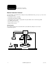
UltraSPARC™-II CPU Module 400 MHz CPU, 4.0 MB E-Cache Advanced Version SME5224AUPA-400 SYSTEM INTERFACE Figure 2 shows the major components of a UPA based uniprocessor system. The system controller [1] for the UPA bus arbitrates between the UltraSPARC™–II, 400 MHz CPU, 4.0 Mbyte module, and the I/O bridge chip. The figure also illustrates a slave-only UPA graphics port for Sun graphics boards . The module UPA system interface signals run at one-quarter of the rate of the internal CPU frequency.
SME5224AUPA-400 UltraSPARC™-II CPU Module 400 MHz CPU, 4.0 MB E-Cache Module ID Module IDs are used to configure the UPA address of a module. The UPA_PORT_ID[4:3] are hardwired on the module to “0”. UPA_PORT_ID[1:0] are brought out to the connector pins. Each module is hardwired in the system to a fixed and unique UPA address. This feature supports systems with four or fewer processors.
UltraSPARC™-II CPU Module 400 MHz CPU, 4.0 MB E-Cache Advanced Version SME5224AUPA-400 SIGNAL DESCRIPTION [1] System Interface Signal Type Name and Function UPA_ADDR[35:0] I/O Packet switched transaction request bus. Maximum of three other masters and one system controller can be connected to this bus. Includes 1-bit odd-parity protection. Synchronous to UPA_CLK. UPA_ADDR_VALID I/O Bidirectional radial UltraSPARC-II Bus signal between the UltraSPARC-II CPU and the system.
UltraSPARC™-II CPU Module 400 MHz CPU, 4.0 MB E-Cache SME5224AUPA-400 JTAG/Debug Interface Signal Type Name and Function O IEEE 1149 test data output. A three-state signal driven only when the TAP controller is in the shift-DR state. TDI I IEEE 1149 test data input. This pin is internally pulled to logic one when not driven. TCK I IEEE 1149 test clock input. This pin if not hooked to a clock source must always be driven to a logic 1 or a logic 0. TMS I IEEE 1149 test mode select input.
UltraSPARC™-II CPU Module 400 MHz CPU, 4.0 MB E-Cache Advanced Version SME5224AUPA-400 UPA AND CPU CLOCKS Module Clocks The module receives three differential pair low voltage PECL (LVPECL) clock signals (CPU_CLK, UPA_CLK0 and UPA_CLK1) from the systemboard and terminates them. The CPU_CLK is unique in the system, but the UPA_CLKs are two of many UPA clock inputs in the system. The CPU_CLK operates at 1/2 the CPU core frequency. The UPA_CLKs operate at the UPA bus frequency.
SME5224AUPA-400 UltraSPARC™-II CPU Module 400 MHz CPU, 4.0 MB E-Cache . Module Boundary CPU_CLK Module Connector Serial Parallel SRAM SRAM UDB-II UPA_CLK0 Clock Generator Clock Buffer UDB-II SRAM SRAM SRAM SRAM SRAM SRAM Clock Divider SRAM/TAG UPA_CLK1 UPA_CLK UltraSPARC-II CPU Clock Buffer UPA_CLK2 UPA_CLKx UPA Device UPA Device Figure 3. Clock Signal Distribution LOW VOLTAGE PECL Two trace signals compose each clock: one positive signal and one negative signal.
Advanced Version UltraSPARC™-II CPU Module 400 MHz CPU, 4.0 MB E-Cache SME5224AUPA-400 ELECTRICAL CHARACTERISTICS Absolute Maximum Ratings [1] Symbol Parameter Rating Units VDD Supply voltage range for I/O 0 to 3.8 V VDD_CORE [2] Supply voltage range for CPU core 0 to 3.0 V VI Input voltage range [3] -0.5 to VDD + 0.5 V VO Output voltage range -0.5 to VDD + 0.
SME5224AUPA-400 UltraSPARC™-II CPU Module 400 MHz CPU, 4.0 MB E-Cache DC Characteristics [1] Parameter Conditions Min Typ Max VOH Symbol High-level output voltage VDD = Min, IOH = Max 2.4 – – V VIH High-level input voltage, PECL clocks, 2.28 – – V High-level input voltage, except PECL clocks 2.0 – – V Low-level input voltage, PECL clocks – – 1.49 V Low-level input voltage, except PECL clocks – – 0.
Advanced Version UltraSPARC™-II CPU Module 400 MHz CPU, 4.0 MB E-Cache SME5224AUPA-400 UPA Data Bus SPICE Model A typical circuit for the UPA data bus and ECC signals is illustrated in Figure 4:. Edge Connector UDB-II Driver Trace 1 3.1 nH Trace 2 1.0 pF 1.0 pF Edge Connector via 0.6 pF 3.1 nH Trace 3 0.5 nH 1.0 pF 1.0 pF via 0.6 pF 2 nH 0.
SME5224AUPA-400 UltraSPARC™-II CPU Module 400 MHz CPU, 4.0 MB E-Cache UPA AC TIMING SPECIFICATIONS The UPA AC Timing Specifications are referenced to the UPA connector. The timing assumes that the clocks are correctly distributed, (see the section "System Clock Distribution," on page 9). The effective PCB clock trace lengths (CPU_CLK, UPA_CLK0 and UPA_CLK1) are used to calculate a balanced clock system.
UltraSPARC™-II CPU Module 400 MHz CPU, 4.0 MB E-Cache Advanced Version SME5224AUPA-400 Setup and Hold Time Specifications 400 MHz CPU 100 MHz UPA Symbol Setup Signals and Hold Time Signals Waveforms Min Max Unit tH UPA_DATA [127:0] 1 0.4 – ns Hold time UPA_ADDR [35:0] UPA_ADDR_VALID, UPA_REQ_IN [2:0], UPA_SC_REQ_IN, UPA_DATA_STALL, UPA_ECC_VALID, UPA_RESET_L, UPA_XIR_L 1 0.4 – ns UPA_ECC [15:0] 1 0.4 – ns UPA_S_REPLY [3:0] 1 0.
SME5224AUPA-400 UltraSPARC™-II CPU Module 400 MHz CPU, 4.0 MB E-Cache MECHANICAL SPECIFICATIONS The module components and dimensions are specified in Figure 6, Figure 7, Figure 8 and Figure 9. Module Ejectors CPU/Voltage Regulator Heat Sink Thermistor Location (RT0201) UDB Heat Sinks Front SRAM Heat Sinks Figure 6. CPU Module Components 6.250 [158.75] 5.890 [149.61] 0.315 [8.00] 0.179 [4.55] 3.680 [93.47] 4.250 [107.95] Pin 328 0.535 [13.59] 0.540 [13.72] 0.570 [14.48] Pin 1 .200 [5.08] 3.
UltraSPARC™-II CPU Module 400 MHz CPU, 4.0 MB E-Cache Advanced Version SME5224AUPA-400 Module Shroud Bidirectional Airflow Bidirectional Airflow Backside SRAM Heat sink Figure 8. CPU Module Side View ,,,,,,,,,,,, ,, ,, ,,,,,,,,,,,, Provide Minimum Frontside Clearance 0.079 [2.00] Maximum Card Guide Depth 0.087 [2.201] 0.298 [7.57] Maximum 1.318 [33.48] Maximum 0.062 + 0.008 [1.57 + 0.20] Provide Minimum 0.079 [2.00] Backside Clearance Dimensions: inches [millimeters] Figure 9.
SME5224AUPA-400 UltraSPARC™-II CPU Module 400 MHz CPU, 4.0 MB E-Cache THERMAL SPECIFICATIONS The maximum CPU operating frequency and I/O timing is reduced when the junction temperature (Tj) of the CPU device is raised. Airflow must be directed to the CPU heatsink to keep the CPU device cool. Correct airflow maintains the junction temperature within its operating range.
UltraSPARC™-II CPU Module 400 MHz CPU, 4.0 MB E-Cache Advanced Version SME5224AUPA-400 Thermal Definitions and Specifications Term Definition Specification Comments Tj Maximum device junction temperature 85 °C, The Tj can't be measured directly by a thermo-couple probe. It must always be estimated as Tj or less. Less is preferred. Tc Maximum case temperature 76.7 °C Measurable at the top-center of the device.
UltraSPARC™-II CPU Module 400 MHz CPU, 4.0 MB E-Cache SME5224AUPA-400 Temperature Estimating and Measuring Methods The following methods can be used to estimate air cooling requirements and calculate junction temperature based on thermo-couple temperature measurements.
UltraSPARC™-II CPU Module 400 MHz CPU, 4.0 MB E-Cache Advanced Version SME5224AUPA-400 Case Temperature Measuring Method The relationship between case temperature and junction temperature is described in the following thermal equation. If Tc is known, then Tj can be calculated: Tj = Tc + (Pd x θjc) Note: Testing is done with the worst-case power draw, software loading, and ambient air temperature. There is good tracking between the case temperature and the heatsink temperature.
SME5224AUPA-400 UltraSPARC™-II CPU Module 400 MHz CPU, 4.0 MB E-Cache JTAG TESTABILITY The UltraSPARC™–II, 400 MHz CPU, 4.0 Mbyte module, (SME5224AUPA-400), implements the IEEE 1149.1 standard to aid in board level testing. Boundary Scan Description Language (BSDL) files are available for all the active devices on the module, except the clock buffer.
UltraSPARC™-II CPU Module 400 MHz CPU, 4.0 MB E-Cache Advanced Version SME5224AUPA-400 JTAG (IEEE 1149.1) TIMING VIH Clock 2.0V VIL tSU tH VIH Data Input 1.5V 1.5V VIL Figure 10. Voltage Waveforms - Setup and Hold Times VIH Clock 2.0V VIL tPD tOH In-Phase Output 2.0V 0.8V tPD tOH Out-of-Phase Output VOH VOL VOH 0.8V VOL Figure 11.
SME5224AUPA-400 UltraSPARC™-II CPU Module 400 MHz CPU, 4.
UltraSPARC™-II CPU Module 400 MHz CPU, 4.
SME5224AUPA-400 UltraSPARC™-II CPU Module 400 MHz CPU, 4.0 MB E-Cache STORAGE AND SHIPPING SPECIFICATION Value Parameter Conditions Min. Typ. Max Unit -40 – 90 °C Temperature Ambient Temperature ramp Ambient – – 10 °C/min.
UltraSPARC™-II CPU Module 400 MHz CPU, 4.0 MB E-Cache Advanced Version SME5224AUPA-400 ORDERING INFORMATION [1] Part Number CPU Speeds SME5224AUPA-400 400 MHz CPU Description The UltraSPARC™–II, 400 MHz CPU, 4.0 Mbyte module, features the UltraSPARC-II CPU at 400 MHz, a 4.0 Mbyte external cache, and two UDB-II data buffer ASICs. 1. To order the data sheet for this device use the document part number: 805-6390-05 DOCUMENT REVISION HISTORY Date Document No.
SME5224AUPA-400 Sun Microsystems, Inc. 901 San Antonio Road Palo Alto, CA 94303-4900 USA 800/681-8845 www.sun.com/microelectronics ©1999 Sun Microsystems, Inc. All Rights reserved. THE INFORMATION CONTAINED IN THIS DOCUMENT IS PROVIDED “AS IS” WITHOUT ANY EXPRESS REPRESENTATIONS OF WARRANTIES. IN ADDITION, SUN MICROSYSTEMS, INC.