Sundance Technology PRELIMINARY draft 2 ST201 Fast Ethernet MAC FEATURES GENERAL DESCRIPTION • Single chip 10/100BASE, half or full duplex Ethernet Media Access Controller • IEEE 802.3u compliant MII • IEEE 802.3x full duplex flow control • PCI Bus master scatter/gather DMA on any byte boundary The ST201 is a single-chip, full duplex, 10/ 100Mbps Ethernet MAC incorporating a 32-bit PCI including bus master support.
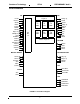
Sundance Technology ST201 PRELIMINARY draft 2 BLOCK DIAGRAM PCI RSTN PCICLK GNTN IDSEL INTAN WAKE REQN AD[31..0] CBEN[3:0] PAR FRAMEN IRDYN TRDYN DEVSELN STOPN PERRN SERRN VDET MII Status/Control Registers Tx Tx DMA PCI Bus I/F FIFO Rx Rx DMA FIFO TXD[3..0] TXEN TXCLK RXD[3..0] RXCLK RXER RXDV CRS COL MDC MDIO Tx MAC Rx MAC Statistic Registers EEPROM EEDO EEDI EESK EECS EXPANSION ROM MISCELLANEOUS ED[7..0] EA[15..
Sundance Technology ST201 PRELIMINARY draft 2 ORDERING INFORMATION Sundance products are available in several combinations of packages and operating temperature ranges.
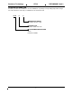
Sundance Technology ST201 PIN DIAGRAM 4 PRELIMINARY draft 2
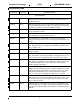
Sundance Technology ST201 PRELIMINARY draft 2 PIN DESIGNATIONS PIN NO. PIN NAME PIN NO. PIN NO. PIN NAME 1 2 3 4 5 6 7 8 VCC (5V) CBEN3 IDSEL AD23 AD22 AD21 AD20 GND (5V) 33 34 35 36 37 38 39 40 AD9 GND (5V) AD8 CBEN0 AD7 AD6 AD5 GND (3.
Sundance Technology ST201 PRELIMINARY draft 2 PIN DESCRIPTIONS PIN NAME PIN TYPE PIN DESCRIPTION PCI INTERFACE RSTN INPUT Reset, asserted LOW. RSTN will cause the ST201 to reset all of its functional blocks. RSTN must be asserted for a minimum duration of 10 PCICLK cycles. PCICLK INPUT PCI Bus Clock. This clock is used to drive the PCI bus interfaces and the internal DMA logic. All bus signals are sampled on the rising edges of PCICLK. PCICLK can operate from 0MHz to 33MHz.
Sundance Technology PIN NAME ST201 PIN TYPE PRELIMINARY draft 2 PIN DESCRIPTION TRDYN IN/OUT Target Ready, asserted LOW. A bus target asserts TRDYN to indicate valid read data phases, and to indicate it is ready to accept data during write data phases. A bus master will monitor TRDYN. DEVSELN IN/OUT Device Select, asserted LOW. The ST201 asserts DEVSELN when it is selected as a target during a bus transaction.
Sundance Technology PIN NAME ST201 PIN TYPE PRELIMINARY draft 2 PIN DESCRIPTION COL INPUT Collision. COL is asserted by the PHY to a signal collision condition is detected on the physical medium. COL is asynchronous to RXCLK and TXCLK. MDC OUTPUT Management Data Clock. MDC is used to synchronize the read and write operations of MDIO. MDIO IN/OUT Management Data Input/Output. MDIO carries management data for the management port read and write operations.
Sundance Technology PIN NAME ST201 PIN TYPE PRELIMINARY draft 2 PIN DESCRIPTION LEDPWRN OUTPUT Power Status LED. (This pin is shared with EA9). The operation of this pin varies based on the setting in the I/O Registers, AsicCtrl bit 14 (the LEDMode bit). In Mode 0, LOW when power is applied, and toggling when frame transmission is in progress. In Mode 1, this pin is always LOW when power is applied. LEDLNKN OUTPUT Link Status LED. (This pin is shared with EA10).
Sundance Technology ST201 ACRONYMS AND GLOSSARY LAN Local Area Network MAC Media Access Control Layer, or a device implementing the functions of this layer (a Media Access Controller) PCI Peripheral Component Interface NIC Network Interface Cards FIFO First In First Out MII Media Independent Interface EPROM Erasable Programmable Only Memory EEPROM Electrically Erasable Programmable Read Only Memory LED Light Emitting Diode PHY Physical Layer, or device implementing functions of the Phys
Sundance Technology ST201 PCI BUS INTERFACE PRELIMINARY draft 2 complete frame must be transferred from the host system memory to the TxFIFO again by TxDMA Logic. The PCI Bus Interface (PBI) implements the procedures and algorithms needed to link the ST201 to a PCI bus. The ST201 can be either a PCI bus master or slave. The PBI is also responsible for managing the DMA interfaces and the host processors access to the ST201 registers.
Sundance Technology ST201 EXPANSION ROM INTERFACE PRELIMINARY draft 2 • loBaseAddress sets the I/O base address for the ST201 registers. • MemBaseAddress sets the memory base address for the ST201 registers. • ExpRomBaseAddress sets the base address and size for an installed expansion ROM, if any. • CacheLineSize indicates the system’s cache line size. This value is used by the ST201 to optimize bus master data transfers.
Sundance Technology ST201 dress register. Setting the ReceiveBroadcast and ReceiveMulticast bits in the ReceiveMode register will allow the ST201 to receive all broadcast and multicast frames, respectively. The ReceiveMulticastHash bit in ReceiveMode enables a filtering mechanism for Ethernet multicast frames. This filtering mechanism uses a 64-bit hash table (HashTable register) for selective reception of Ethernet multicast frames.
Sundance Technology ST201 PRELIMINARY draft 2 The resulting linked list of TFDs is referred to as the TxDMAList, as shown in Figure 3. TXDMA AND FRAME TRANSMISSION The TxDMA block transfers frame data from a host system to the ST201 based on a linked list of frame descriptors called TFDs. The frame to be transmitted is divided into data fragments (or buffers) within the host system’s memory.
Sundance Technology ST201 The TxDMAListPtr I/O register within the ST201 contains the physical address that points to the head of the TxDMAList. TxDMAListPtr must point to addresses which are on 8-byte boundaries. A value of zero in the TxDMAListPtr register implies there are no pending TFD’s for the ST201 to process. PRELIMINARY draft 2 probably set TxDMAIndicate to generate an interrupt.
Sundance Technology ST201 are independent of each other in general. A special case is when a transmit under run occurs. In this case the current frame being transmitted is the only frame in the TxFIFO. When a transmit under run occurs, the ST201 stops TxDMA operation and generates an interrupt with a TxUnderrun error flagged in TxStatus. The host system can determine which is the under run error frame by examining the current value of TxDMAListPtr.
Sundance Technology ST201 PRELIMINARY draft 2 tions. Similar to TxDMA, the RxDMA Logic can be controlled by the RxDMAHalt and RxDMAResume bits. The host system should set the RxDMAHalt bit before modifying the list pointers in the RxDMAList. The RxDMA Logic will return to the idle state when the RxDMAListPtr register is zero. received and transferred by RxDMA, a RxDMAComplete interrupt will be generated for each frame.
Sundance Technology ST201 Systems using the ST201 can be programmed to generate an interrupt based upon the number of bytes that have been received in a frame. The RxEarlyThresh register sets the value for early receive threshold. As soon as the number of bytes that have been received is greater than the value in RxEarlyThresh register, the ST201 will generate a RxEarly interrupt, if it is enabled, to the host. The RxEarly interrupt will only occur when the frame being received is the top frame, i.e.
Sundance Technology ST201 STATISTICS PRELIMINARY draft 2 this statistic. • CarrierSenseErrors: Frames that were transmitted without error but experienced a loss of carrier are counted by this statistic. The ST201 implements 16 statistics counters of various widths. Each statistic implemented complies to the corresponding definition given in the IEEE 802.3 standard. Setting the StatisticsEnable bit in the MACCtrl register enables the gathering of statistics.
Sundance Technology ST201 disable the use of MWI and MRL. MWIDisable and MRLDisable are cleared by default, enabling MWI and MRL. PRELIMINARY draft 2 ST201 optionally supports this state determined by the D1Support bit in the ConfigParm word in EEPROM. The D1 state allows transition back to D0 with no delay. In this state, the ST201 responds to PCI configuration accesses, to allow the system to change the power state. In D1 the ST201 does not respond to any PCI I/O or memory accesses.
Sundance Technology ST201 D1, D2, or D3. When the ST201 detects a Wake Packet, it signals a wake event on PMEN (if PMEN assertion is enabled), and sets the WakePktEvent bit in the WakeEvent register. The ST201 can signal that a wake event has occurred when it receives a pre-defined frame from another station. The host system transfers a set of frame data patterns into the TxFIFO using the TxDMA function before placing the ST201 in a power-down state.
Sundance Technology ST201 network via transmission of a special frame. Once the ST201 has been placed in Magic Packet mode and put to sleep, it scans all incoming frames addressed to it for a data sequence consisting of 16 consecutive repetitions of its own 48-bit Ethernet MAC StationAddress. This sequence can be located anywhere within the frame, but must be preceded by a synchronization stream. The synchronization stream is defined as 6 bytes of 0xFF.
Sundance Technology 3. 4. 5. ST201 Set MgmtClk Write the desired data bit to MgmtData Wait a minimum of 200 ns 7. 8. To perform a Z cycle used during the Turnaround portion of a register read frame, the host system should follow the procedure below. 1. Clear MgmtClk 2. Wait a minimum of 200 ns 3. Set MgmtClk 4. Clear MgmtDir 5. Wait a minimum of 200 ns 9. PRELIMINARY draft 2 written within the PHY device. Execute 2 write cycles to transmit the 2 bit Write Turnaround value of 0x02.
Sundance Technology 8. 9. ST201 Verify EepromBusy is false. Issue WriteRegister command (opcode = 01 aaaa aaaa) 4. 5. Step 4 through 8 may be skipped for certain types of EEPROM devices. 6. ADAPTER TXDMA SEQUENCE Beginning with the host system writing to the TxDMAListPtr register (when starting from an empty TxDMAList, for instance), the ST201 performs the following procedure during transfers of TxDMA frames. 1. Verifies the TxDMAListPtr is non-zero. 2. Verifies not in the TxDMAHalt state. 3.
Sundance Technology 4. 5. ST201 tion of the “first TFD” in the TxDMAList. Restore the TxDMANextPtr of the “first TFD”, and restart this process. Copy the value of the “first TFD’s” TxDMANextPtr into the TxDMANextPtr field of the inserted TFD. Update the TxDMANextPtr field of the “first TFD” with the address of the inserted TFD. 9. 10. 11. TRANSMIT INTERRUPT OPTIMIZATIONS The transmit mechanism can be optimized by the host system, allowing a reduction in the number of interrupts generated.
Sundance Technology ST201 host system then returns to the operating system an indication of readiness to be powered down (making sure to leave the ReceiveMode register set to receive the appropriate Wake/ Magic packets). The operating system eventually writes to the PowerMgmtCtrl register, placing the ST201 in one of the power down states, and enabling PMEN assertion, while the ST201 monitors for the occurrence of enabled wake events.
Sundance Technology ST201 PRELIMINARY draft 2 REGISTERS AND DATA STRUCTURES DMA DATA STRUCTURES A TFD is used to move data, which is to be transmitted onto a LAN, from host system memory to the TxFIFO within the ST201. A TFD is 16 to 512 bytes in length, and it’s location in host system memory is indicated by the value in the TxDMAListPtr register. A RFD is used to move data, which has been received from a LAN, from the RxFIFO within the ST201 to host system memory.
Sundance Technology ST201 PRELIMINARY draft 2 TXDMAFRAGADDR Class....................DMA Data Structures, TFD Base Address ......Start of TFD Address Offset .....0x00+n·8 for nth fragment Access Mode .......Read/Write Width ...................32 bits BIT 31..0 BIT NAME TxDMAFragAddr BIT DESCRIPTION Transmit Fragment Address contains the physical address of a contiguous block of data to be transferred by TxDMA into the ST201 and transmitted. A fragment can start on any byte boundary.
Sundance Technology ST201 PRELIMINARY draft 2 TXDMAFRAGLEN Class....................DMA Data Structures, TFD Base Address ......Start of TFD Address Offset .....0x04+n·8 for nth fragment Access Mode .......Read/Write Width ...................32 bits Transmit Fragment Length (TxDMAFragLen) contains fragment length and control information for the block of data pointed to by the corresponding TxDMAFragAddr. BIT BIT NAME BIT DESCRIPTION 12..
Sundance Technology ST201 PRELIMINARY draft 2 TXDMANEXTPTR Class....................DMA Data Structures, TFD Base Address ......Start of TFD Address Offset .....0x00 Access Mode .......Read/Write Width ...................32 bits BIT BIT NAME 31..0 TxDMANextPtr BIT DESCRIPTION Transmit Next Pointer, the first double word in the TFD contains the physical address of the next TFD in the TxDMAList.
Sundance Technology ST201 PRELIMINARY draft 2 TXFRAMECONTROL Class....................DMA Data Structures, TFD Base Address ......Start of TFD Address Offset .....0x04 Access Mode .......Read/Write Width ...................32 bits TxFrameControl contains frame control information for the TxDMA function and the transmit function. BIT BIT NAME BIT DESCRIPTION 1..
Sundance Technology ST201 PRELIMINARY draft 2 RXDMANEXTPTR Class....................DMA Data Structures, RFD Base Address ......Start of RFD Address Offset .....0x00 Access Mode .......Read/Write Width ...................32 bits BIT BIT NAME 31..0 RxDMANextPtr BIT DESCRIPTION The first dword in the RFD contains the physical address of the next RFD in the RxDMAList. If this is the last RFD in the RxDMAList, then this value must be zero. RFDs must be aligned on 8-byte physical address boundaries.
Sundance Technology ST201 PRELIMINARY draft 2 RXFRAMESTATUS Class....................DMA Data Structures, RFD Base Address ......Start of RFD Address Offset .....0x04 Access Mode .......Read/Write Width ...................32 bits The second dword in the RFD is ReceiveFrameStatus. At the end of a RxDMA frame transfer, the ST201 writes the value of the RxDMAStatus register into this location in the RFD. The bit definitions for TxFrameStatus for bits[31..29] and [27..
Sundance Technology BIT ST201 BIT NAME PRELIMINARY draft 2 BIT DESCRIPTION 22..21 Reserved Reserved for future use. Should be set to 0. 23 DribbleBits Indicates that the frame had accompanying dribble bits. This bit is informational only, and does not indicate a frame error. 24 RxDMAOverflow Indicates that the RFD had insufficient buffer space for the frame data and there were still data left to be transferred by RxDMA when the ST201 ran out of fragment space.
Sundance Technology ST201 PRELIMINARY draft 2 RXDMAFRAGADDR Class....................DMA Data Structures, RFD Base Address ......Start of RFD Address Offset .....0x00+n·8 for nth fragment Access Mode .......Read/Write Width ...................32 bits BIT 31..0 BIT NAME RxDMAFragAddr BIT DESCRIPTION The third and all subsequent odd dwords in the RFD contains the physical address of a contiguous block of system memory to which receive data is to be transferred by RxDMA.
Sundance Technology ST201 PRELIMINARY draft 2 RXDMAFRAGLEN Class....................DMA Data Structures, RFD Base Address ......Start of RFD Address Offset .....0x04+n·8 for nth fragment Access Mode .......Read/Write Width ...................32 bits The fourth and all subsequent even dwords in the RFD contains fragment length and control information for the block of data pointed to by the previous RxDMAFragAddr. BIT BIT NAME BIT DESCRIPTION 12..
Sundance Technology ST201 PRELIMINARY draft 2 WAKE EVENT DATA STRUCTURES The first Wake Event Data Structure is the Pseudo Packet. A Pseudo Packet is a set of patterns loaded into the ST201 TxFIFO which specify bytes to be examined within received frames. A CRC is calculated over these bytes and compared with a CRC value supplied in the Pseudo Packet. If a match is found, the ST201 issues a Wake Event. The matching technique may result in false wake events being reported to the host system.
Sundance Technology ST201 PRELIMINARY draft 2 PSEUDOPATTERN Class....................Wake Event Data Structures, Pseudo Packet Base Address ......Start of Pseudo Packet Address Offset .....0x00 thru 0x00+n-1 for nth PseudoPattern Access Mode .......Write only Width ...................8 bits BIT BIT NAME BIT DESCRIPTION 3..0 ByteCount ByteCount can take on a value of 0x0 to 0xe. A value of 0xf indicates an extended value.
Sundance Technology ST201 PRELIMINARY draft 2 TERMINATOR Class....................Wake Event Data Structures, Pseudo Packet Base Address ......Start of Pseudo Packet Address Offset .....0x00+n for n PseudoPattern Access Mode .......Write only Width ...................8 bits BIT 7..0 BIT NAME Terminator BIT DESCRIPTION A value of 0x00 indicates the end of the PseudoPattern.
Sundance Technology ST201 PRELIMINARY draft 2 PSEUDOCRC Class....................Wake Event Data Structures, Pseudo Packet Base Address ......Start of Pseudo Packet Address Offset .....0x00+n+1 for n PseudoPatterns Access Mode .......Write only Width ...................32 bits The 32-bit CRC as defined in the IEEE 802.3 Ethernet standard for the FCS, taken over the bytes (indicated by the PseudoPattern values) of a received frame. BIT BIT NAME BIT DESCRIPTION 7..
Sundance Technology ST201 PRELIMINARY draft 2 MAGICSYNCSTREAM Class....................Wake Event Data Structures, Magic Packet Base Address ......Start of Magic Packet Address Offset .....0x00 Access Mode .......Read only Width ...................48 bits BIT 47..0 BIT NAME BIT DESCRIPTION MagicSyncStream A stream of 6 bytes with the value 0xff indicates the start of the MagicSequence.
Sundance Technology ST201 PRELIMINARY draft 2 MAGICSEQUENCE Class....................Wake Event Data Structures, Magic Packet Base Address ......Start of Magic Packet Address Offset .....0x06 Access Mode .......Read only Width ...................768 bits BIT 767..0 BIT NAME MagicSequence BIT DESCRIPTION A sequence of 96 bytes, consisting of 16 consecutive, identical 6 bytes sequences, where each 6 byte sequence equals the station address of the station receiving the Magic Packet.
Sundance Technology ST201 PRELIMINARY draft 2 I/O REGISTERS The host interacts with the ST201 mainly through slave registers, which occupy 128 bytes in the host system’s I/O space, memory space, or both. Generally, registers are referred to as “I/O registers”, implying that the registers may in fact be mapped and accessed by the host system in memory space. I/O registers must be accessed with instructions that are no larger than the bit-width of that register.
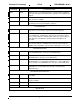
Sundance Technology ST201 PRELIMINARY draft 2 byte 3 byte 2 byte 1 byte 0 Offset McstFramesRcvdOk McstFramesXmtdOk BcstFramesRcvdOk BcstFramesXmtdOk 0x7c FramesAbortXSColls FramesWEXDeferral FramesLostRxErrors FramesWDeferedXmt 0x78 SingleColFrames MultipleColFrames LateCollisions CarrierSenseErrors 0x74 FramesReceivedOk FramesTransmittedOk 0x70 OctetsTransmittedOk(1) OctetsTransmittedOk(0) 0x6c OctetsReceivedOk(1) OctetsReceivedOk(0) 0x68 HashTable(3) HashTable(2) 0x64 Ha
Sundance Technology ST201 PRELIMINARY draft 2 ASICCTRL Class....................I/O Registers, Control and Status Base Address ......IoBaseAddress register value Address Offset .....0x30 Access Mode .......Read/Write Width ...................32 bits AsicCtrl provides chip-specific, non-host-related settings. The contents of the least significant byte of AsicCtrl are read from EEPROM at reset. BIT BIT NAME BIT DESCRIPTION 0 Reserved Reserved for future use. Should be set to 0.
Sundance Technology BIT ST201 BIT NAME PRELIMINARY draft 2 BIT DESCRIPTION 10..8 ForcedConfig These bits are used to place the ST201 into Forced Configuration mode. The bit values are latched in from ED[2..0] pins with a logic inversion at the end of RSTN or power on reset. 000: no forced configuration 001: forced configuration mode 1 010-111: reserved Note: When ForcedConfig[10] is set, the ST201 will use an alternate DeviceID and VendorID.
Sundance Technology BIT ST201 BIT NAME PRELIMINARY draft 2 BIT DESCRIPTION 19 DMA When set, together with GlobalReset, RxReset, or TxReset bits, will reset RxDMA and TxDMA Logic, including: TxDMAListPtr, RxDMAListPtr, TxDMAComplete TxDMAInProg RxDMAComplete and RxEarlyEnable in DMACtrl and RxDMAStatus. When cleared, reset will not have action on the DMA Logic. This bit is self-clearing. Setting this bit has no meaning if the corresponding reset bits are not set.
Sundance Technology ST201 PRELIMINARY draft 2 DEBUGCTRL Class....................I/O Registers, Control and Status Base Address ......IoBaseAddress register value Address Offset .....0x1a Access Mode .......Read/Write Width ...................16 bits DebugCtrl selects the functions of the GPIO pins. DebugCtrl is cleared by reset. BIT BIT NAME BIT DESCRIPTION 0 GPIO0Ctrl This bit controls the GPIO0 pin. When cleared, GPIO0 pin is an input. When set, GPIO0 pin is an output.
Sundance Technology ST201 PRELIMINARY draft 2 HASHTABLE Class....................I/O Registers, Control and Status Base Address ......IoBaseAddress register value Address Offset .....0x66, 0x64, 0x62, 0x60 Access Mode .......Read/Write Width ...................64 bits (accessible as 4, 16 bit words) The host stores the 64-bit hash table in this register for selectively receiving multicast frames. Setting the ReceiveMulticastHash bit in ReceiveMode enables the filtering mechanism.
Sundance Technology ST201 PRELIMINARY draft 2 MACCTRL Class....................I/O Registers, Control and Status Base Address ......IoBaseAddress register value Address Offset .....0x50 Access Mode .......Read/Write Width ...................32 bits This register provides for setting of MAC-specific parameters. It is cleared upon reset. BIT 1..0 BIT NAME IFSSelect BIT DESCRIPTION This field is used to select the size of Inter-Frame Spacing (IFS).
Sundance Technology BIT ST201 BIT NAME PRELIMINARY draft 2 BIT DESCRIPTION 9 RcvFCS This bit is set by the host if it is desired for the receive frame’s FCS to be passed to the host as part of the data in the RxFIFO. The state of RcvFCS does not affect the ST201’s checking of the frame’s FCS and its posting of FCS error status. RcvFCS is cleared by a system reset. To avoid confusing the RxFIFO logic, the value of RcvFCS should only be changed when the receiver is disabled and the RxFIFO is empty.
Sundance Technology BIT ST201 BIT NAME PRELIMINARY draft 2 BIT DESCRIPTION 30 Paused This read-only status bit is set by ST201 to indicate that a PAUSE MAC Control frame had been received and halted the transmit MAC for the duration of the pause_time. It is cleared when the MAC can resume transmission. 31 Reserved Reserved for future use. Should be set to 0. The loopback modes available to a host system when using the ST201 are shown in Table 3.
Sundance Technology ST201 PRELIMINARY draft 2 MAXFRAMESIZE Class....................I/O Registers, Control and Status Base Address ......IoBaseAddress register value Address Offset .....0x5a Access Mode .......Read/Write Width ...................16 bits Sets the maximum frame size for received frames. BIT BIT NAME 15..0 MaxFrameSize BIT DESCRIPTION Received frames with sizes equal to or larger than the value in MaxFrameSize will be flagged as oversize by RxOversizedFrame bit in RxDMAStatus.
Sundance Technology ST201 PRELIMINARY draft 2 RECEIVEMODE Class....................I/O Registers, Control and Status Base Address ......IoBaseAddress register value Address Offset .....0x5c Access Mode .......Read/Write Width ...................8 bits Each bit in ReceiveMode, when set, enables reception of a different type of frame. ReceiveMode is cleared upon reset.
Sundance Technology ST201 PRELIMINARY draft 2 STATIONADDRESS Class....................I/O Registers, Control and Status Base Address ......IoBaseAddress register value Address Offset .....0x47 Access Mode .......Read/Write Width ...................8 bits StationAddress is used to define the individual destination address that the ST201 will respond to when receiving frames.
Sundance Technology ST201 PRELIMINARY draft 2 TXFRAMEID Class....................I/O Registers, Control and Status Base Address ......IoBaseAddress register value Address Offset .....0x5c Access Mode .......Read Width ...................8 bits TxFrameId contains the frame ID for the currently transmitting or most recently transmitted frame. BIT 7..0 BIT NAME TxFrameId BIT DESCRIPTION This register contains the value from FrameId sub-field within the frame’s TFD, TransmitFrameControl field.
Sundance Technology ST201 PRELIMINARY draft 2 TXSTATUS Class....................I/O Registers, Control and Status Base Address ......IoBaseAddress register value Address Offset .....0x46 Access Mode .......Read (write to advance queue) Width ...................8 bits The TxStatus register returns the status of frame transmission or transmission attempts. TxStatus actually implements a queue of up to 31 transmit status bytes.
Sundance Technology ST201 PRELIMINARY draft 2 WAKEEVENT Class....................I/O Registers, Control and Status Base Address ......IoBaseAddress register value Address Offset .....0x45 Access Mode .......Read/Write Width ...................8 bits WakeEvent contains enable bits to control which types of events can generate a wake event to the host system. It also contains status bits indicating the specific events that have occurred.
Sundance Technology ST201 PRELIMINARY draft 2 FIFOCTRL Class....................I/O Registers, FIFO Control Base Address ......IoBaseAddress register value Address Offset .....0x3a Access Mode .......Read/Write Width ...................16 bits The bits in this register provide various control and indications of TxFIFO and RxFIFO diagnostic. BIT BIT NAME BIT DESCRIPTION 0 RAMTestMode When set, the FIFO RAM is in the test mode. This bit is cleared after reset. 8..1 Reserved Reserved for future use.
Sundance Technology ST201 PRELIMINARY draft 2 RXEARLYTHRESH Class....................I/O Registers, FIFO Control Base Address ......IoBaseAddress register value Address Offset .....0x3e Access Mode .......Read/Write Width ...................16 bits The value stored in this register defines the number of bytes of the top of the frame that must be received before a RxEarly interrupt will occur. The first byte of the destination address is considered to be byte 1.
Sundance Technology ST201 PRELIMINARY draft 2 TXRELEASETHRESH Class....................I/O Registers, FIFO Control Base Address ......IoBaseAddress register value Address Offset .....0x5d Access Mode .......Read/Write Width ...................8 bits The value in TxReleaseThresh determines how much data of a frame must be transmitted before the TxFIFO space can be released for use by another frame.
Sundance Technology ST201 PRELIMINARY draft 2 TXSTARTTHRESH Class....................I/O Registers, FIFO Control Base Address ......IoBaseAddress register value Address Offset .....0x3c Access Mode .......Read/Write Width ...................16 bits The value in TxStartThresh is used to control when frames are transmitted. Transmission of a frame begins when the number of bytes for the frame transferred into the TxFIFO is greater than the value in TxStartThresh .
Sundance Technology ST201 PRELIMINARY draft 2 COUNTDOWN Class....................I/O Registers, Interrupt Base Address ......IoBaseAddress register value Address Offset .....0x48 Access Mode .......Read/Write Width ...................16 bits Countdown is a programmable down-counter that will generate an interrupt upon its expiration. If the CountdownIntEnable bit in DMACtrl is set, the IntRequested interrupt will be generated when Countdown counts through zero.
Sundance Technology ST201 PRELIMINARY draft 2 INTENABLE Class....................I/O Registers, Interrupt Base Address ......IoBaseAddress register value Address Offset .....0x4c Access Mode .......Read/Write Width ...................16 bits Enables individual interrupts as specified in the IntStatus register. Setting a bit in IntEnable will allow the specific source to generate an interrupt on the PCI bus. IntEnable is cleared upon reset. IntEnable is also cleared by a read of IntStatusAck.
Sundance Technology ST201 PRELIMINARY draft 2 INTSTATUS Class....................I/O Registers, Interrupt Base Address ......IoBaseAddress register value Address Offset .....0x4e Access Mode .......Read/Write Width ...................16 bits IntStatus register indicates the source of interrupts and indications on the ST201. Bits 1 through 10 are the interrupt-causing sources for the ST201. These bits can be individually disabled as interrupt sources using the IntEnable register.
Sundance Technology BIT ST201 BIT NAME PRELIMINARY draft 2 BIT DESCRIPTION 9 TxDMAComplete This bit indicates that a frame TxDMA has completed, and the TFD in question had the TxDMAIndicate bit in its TFC set. This bit can be acknowledged by writing a 1 to this bit. The host should examine the TxDMAListPtr to determine which frame(s) have been transferred by TxDMA. Those frames in the TxDMAList before the current TxDMAListPtr have already been transferred by TxDMA.
Sundance Technology ST201 PRELIMINARY draft 2 INTSTATUSACK Class....................I/O Registers, Interrupt Base Address ......IoBaseAddress register value Address Offset .....0x4a Access Mode .......Read only Width ...................16 bits IntStatusAck is another version of the IntStatus register, having the same bit definition as IntStatus, but providing additional functionality to reduce the number of I/O operations required to perform common tasks related to interrupt handling.
Sundance Technology BIT ST201 BIT NAME PRELIMINARY draft 2 BIT DESCRIPTION 9 TxDMAComplete This bit indicates that a frame TxDMA has completed, and the TFD in question had the TxDMAIndicate bit in its TFC set. This bit can be acknowledged by writing a 1 to this bit. The host should examine the TxDMAListPtr to determine which frame(s) have been transferred by TxDMA. Those frames in the TxDMAList before the current TxDMAListPtr have already been transferred by TxDMA.
Sundance Technology ST201 PRELIMINARY draft 2 DMACTRL Class....................I/O Registers, DMA Base Address ......IoBaseAddress register value Address Offset .....0x00 Access Mode .......Read/Write Width ...................32 bits DMACtrl controls some of the bus master functions in the RxDMA and TxDMA engines, and contains status bits. DMACtrl is cleared by a reset.
Sundance Technology BIT ST201 BIT NAME PRELIMINARY draft 2 BIT DESCRIPTION 15 DMAHaltBusy This read-only bit indicates that a DMA Halt operation (TxDMAHalt or RxDMAHalt) is in progress and the drivers should wait for this bit to be cleared before performing other actions. 16 Reserved Reserved for future use. Should be set to 0. 17 RxEarlyEnable This read/write bit determines when the ST201 may start RxDMA a receive frame.
Sundance Technology BIT 31 ST201 BIT NAME MasterAbort PRELIMINARY draft 2 BIT DESCRIPTION This read-only bit is set when the ST201 experiences a master abort sequence when operating as a bus master. This bit indicates a fatal error, and must be cleared before further TxDMA or RxDMA operation can proceed. This bit is cleared by the GlobalReset/DMA bit.
Sundance Technology ST201 PRELIMINARY draft 2 RXDMABURSTTHRESH Class....................I/O Registers, DMA Base Address ......IoBaseAddress register value Address Offset .....0x14 Access Mode .......Read/Write Width ...................8 bits RxDMABurstThresh sets the threshold when the ST201 makes RxDMA bus master requests, based upon the number of used bytes in the RxFIFO, in units of 32 bytes. When the used space exceeds the threshold, the ST201 may make a RxDMA request on the PCI bus.
Sundance Technology ST201 PRELIMINARY draft 2 RXDMALISTPTR Class....................I/O Registers, DMA Base Address ......IoBaseAddress register value Address Offset .....0x10 Access Mode .......Read/Write Width ...................32 bits RxDMAListPtr holds the physical address of the current RxDMA Frame Descriptor in the RxDMAList. A value of zero in RxDMAListPtr indicates that no more RFDs are available to accept receive frames.
Sundance Technology ST201 PRELIMINARY draft 2 RXDMASTATUS Class....................I/O Registers, DMA Base Address ......IoBaseAddress register value Address Offset .....0x0c Access Mode .......Read only Width ...................32 bits RxDMAStatus shows the status of various operations in the RxDMA Logic. Host systems should read this register only while the RxDMA engine is in the RxDMAHalt state. Otherwise the ST201 may change RFDs between accesses to this register.
Sundance Technology BIT ST201 PRELIMINARY draft 2 BIT NAME BIT DESCRIPTION 20 RxOversizedFrame Indicates the frame size was equal to or greater than the value set in the MaxFrameSize register. This bit is undefined until RxDMAComplete bit is set. 22..21 Reserved Reserved for future use. Should be set to 0. 23 DribbleBits Indicates that the frame had accompanying dribble bits. This bit is informational only, and does not indicate a frame error.
Sundance Technology ST201 PRELIMINARY draft 2 RXDMAPOLLPERIOD Class....................I/O Registers, DMA Base Address ......IoBaseAddress register value Address Offset .....0x16 Access Mode .......Read/Write Width ...................8 bits The value in RxDMAPollPeriod determines the rate at which the current RFD is polled, looking for RxDMAComplete in ReceiveFrameStatus in RFD to be cleared. Polling is disabled when RxDMAPollPeriod is cleared. RxDMAPollPeriod is cleared by reset.
Sundance Technology ST201 PRELIMINARY draft 2 RXDMAURGENTTHRESH Class....................I/O Registers, DMA Base Address ......IoBaseAddress register value Address Offset .....0x15 Access Mode .......Read/Write Width ...................8 bits The value in RxDMAUrgentThresh sets a threshold at which the RxDMA engine will make a urgent bus master request. A urgent RxDMA request will have priority over all other requests on the ST201.
Sundance Technology ST201 PRELIMINARY draft 2 TXDMABURSTTHRESH Class....................I/O Registers, DMA Base Address ......IoBaseAddress register value Address Offset .....0x08 Access Mode .......Read/Write Width ...................8 bits TxDMABurstThresh determines the threshold for when the ST201 makes TxDMA bus master requests, based upon the available space in the TxFIFO. The value in TxDMABurstThresh represents free space in the TxFIFO in multiples of 32 bytes.
Sundance Technology ST201 PRELIMINARY draft 2 TXDMALISTPTR Class....................I/O Registers, DMA Base Address ......IoBaseAddress register value Address Offset .....0x04 Access Mode .......Read/Write Width ...................32 bits TxDMAListPtr holds the physical address of the current TxDMA Frame Descriptor in the TxDMAList. A value of zero in TxDMAListPtr is interpreted by the ST201 to mean that no more frames remain to be transferred by TxDMA.
Sundance Technology ST201 PRELIMINARY draft 2 TXDMAPOLLPERIOD Class....................I/O Registers, DMA Base Address ......IoBaseAddress register value Address Offset .....0x0a Access Mode .......Read/Write Width ...................8 bits The value in TxDMAPollPeriod determines the interval at which the current TFD is polled. When a zero TxDMANextPtr is fetched from the current TFD, TxDMANextPtr is polled to determine when a new TFD is ready to be processed.
Sundance Technology ST201 PRELIMINARY draft 2 TXDMAURGENTTHRESH Class....................I/O Registers, DMA Base Address ......IoBaseAddress register value Address Offset .....0x09 Access Mode .......Read/Write Width ...................8 bits When the number of used bytes in the TxFIFO falls below the value in the TxDMAUrgentThresh, the TxDMA Logic will make an urgent bus master request. An urgent TxDMA request will have priority over the RxDMA, unless it is also making an urgent request.
Sundance Technology ST201 PRELIMINARY draft 2 EEPROMCTRL Class....................I/O Registers, External Interface Control Base Address ......IoBaseAddress register value Address Offset .....0x36 Access Mode .......Read/Write Width ...................16 bits EepromCtrl provides the host with a method for issuing commands to the ST201’s serial EEPROM controller. Individual 16-bit word locations within the EEPROM may be written, read or erased.
Sundance Technology ST201 PRELIMINARY draft 2 EEPROMDATA Class....................I/O Registers, External Interface Control Base Address ......IoBaseAddress register value Address Offset .....0x34 Access Mode .......Read/Write Width ...................16 bits EepromData is a 16-bit data register for use with the adapter’s serial EEPROM. Data from the EEPROM can be read by the host from EepromData register after EepromBusy is cleared.
Sundance Technology ST201 PRELIMINARY draft 2 EXPROMADDR Class....................I/O Registers, External Interface Control Base Address ......IoBaseAddress register value Address Offset .....0x40 Access Mode .......Read/Write Width ...................32 bits ExpRomAddr holds the address to be used for direct I/O accesses of the Expansion ROM through the ExpRomData port. To access a byte in the Expansion ROM, write the address of the byte to be accessed into ExpRomAddr.
Sundance Technology ST201 PRELIMINARY draft 2 EXPROMDATA Class....................I/O Registers, External Interface Control Base Address ......IoBaseAddress register value Address Offset .....0x44 Access Mode .......Read/Write Width ...................8 bits ExpRomData is the data port for performing direct I/O byte-wide accesses of the Expansion ROM. A read of ExpRomData returns the ROM byte value from the location specified by ExpRomAddr.
Sundance Technology ST201 PRELIMINARY draft 2 PHYCTRL Class....................I/O Registers, External Interface Control Base Address ......IoBaseAddress register value Address Offset .....0x5e Access Mode .......Read/Write Width ...................8 bits This register contains control bits for the MII Management Interface. The MII Management Interface is used to access registers in an MII PHY device.
Sundance Technology ST201 PRELIMINARY draft 2 STATISTICS Reading a statistic register will clear it. The statistics gathering must be enabled by setting the StatisticsEnable bit in MACCtrl for the statistics registers to count events. BROADCASTFRAMESRECEIVEDOK Class....................I/O Registers, Statistics Base Address ......IoBaseAddress register value Address Offset .....0x7d Access Mode .......Read (also clears register)/Write Width ...................8 bits BIT 7..
Sundance Technology ST201 PRELIMINARY draft 2 BROADCASTFRAMESTRANSMITTEDOK Class....................I/O Registers, Statistics Base Address ......IoBaseAddress register value Address Offset .....0x7c Access Mode .......Read (also clears register)/Write Width ...................8 bits BIT 7..0 BIT NAME BIT DESCRIPTION BroadcastFramesTransmittedOk This statistic counts the number of frames that are successfully transmitted to the broadcast address.
Sundance Technology ST201 PRELIMINARY draft 2 CARRIERSENSEERRORS Class....................I/O Registers, Statistics Base Address ......IoBaseAddress register value Address Offset .....0x74 Access Mode .......Read (also clears register)/Write Width ...................8 bits BIT BIT NAME BIT DESCRIPTION 3..0 CarrierSenseErrors This statistic register counts the number of times that carrier_sense was not asserted or was de-asserted during the transmission of a frame without collision.
Sundance Technology ST201 PRELIMINARY draft 2 FRAMESABORTEDDUETOXSCOLLS Class....................I/O Registers, Statistics Base Address ......IoBaseAddress register value Address Offset .....0x7b Access Mode .......Read (also clears register)/Write Width ...................8 bits BIT 7..0 BIT NAME BIT DESCRIPTION FramesAbortedDueToXSColls This statistic counts the number of frames that, due to excessive collisions, are not transmitted successfully.
Sundance Technology ST201 PRELIMINARY draft 2 FRAMESLOSTRXERRORS Class....................I/O Registers, Statistics Base Address ......IoBaseAddress register value Address Offset .....0x79 Access Mode .......Read (also clears register)/Write Width ...................8 bits BIT 7..
Sundance Technology ST201 PRELIMINARY draft 2 FRAMESRECEIVEDOK Class....................I/O Registers, Statistics Base Address ......IoBaseAddress register value Address Offset .....0x72 Access Mode .......Read (also clears register)/Write Width ...................16 bits BIT 7..0 BIT NAME FramesReceivedOk BIT DESCRIPTION This statistic counts the number of frames that are successfully received.
Sundance Technology ST201 PRELIMINARY draft 2 FRAMESTRANSMITTEDOK Class....................I/O Registers, Statistics Base Address ......IoBaseAddress register value Address Offset .....0x70 Access Mode .......Read (also clears register)/Write Width ...................16 bits BIT 7..0 BIT NAME BIT DESCRIPTION FramesTransmittedOk This statistic counts the number of frames that are successfully transmitted. This is a 16-bit counter and will wrap around to zero after reaching ffffh.
Sundance Technology ST201 PRELIMINARY draft 2 FRAMESWITHDEFERREDXMISSION Class....................I/O Registers, Statistics Base Address ......IoBaseAddress register value Address Offset .....0x78 Access Mode .......Read (also clears register)/Write Width ...................8 bits BIT 7..0 BIT NAME FramesWithDeferredXmission BIT DESCRIPTION This statistic counts the number of frames that must delay its first attempt of transmission because the medium was busy.
Sundance Technology ST201 PRELIMINARY draft 2 FRAMESWITHEXCESSIVEDEFERAL Class....................I/O Registers, Statistics Base Address ......IoBaseAddress register value Address Offset .....0x7a Access Mode .......Read (also clears register)/Write Width ...................8 bits BIT 7..0 BIT NAME BIT DESCRIPTION FramesWithExcessiveDeferal This statistic counts the number of frames that deferred for an excessive period of time (exceeding the defer limit).
Sundance Technology ST201 PRELIMINARY draft 2 LATECOLLISIONS Class....................I/O Registers, Statistics Base Address ......IoBaseAddress register value Address Offset .....0x75 Access Mode .......Read (also clears register)/Write Width ...................8 bits BIT 7..0 BIT NAME LateCollisions BIT DESCRIPTION This statistic counts the number of times that a collision has been detected later than 512 BT into the transmitted frame.
Sundance Technology ST201 PRELIMINARY draft 2 MULTICASTFRAMESRECEIVEDOK Class....................I/O Registers, Statistics Base Address ......IoBaseAddress register value Address Offset .....0x7f Access Mode .......Read (also clears register)/Write Width ...................8 bits BIT 7..0 BIT NAME MulticastFramesReceivedOk BIT DESCRIPTION This statistic counts the number of frames that are successfully received and are directed to an active non-broadcast group address.
Sundance Technology ST201 PRELIMINARY draft 2 MULTICASTFRAMESTRANSMITTEDOK Class....................I/O Registers, Statistics Base Address ......IoBaseAddress register value Address Offset .....0x7e Access Mode .......Read (also clears register)/Write Width ...................8 bits BIT 7..0 BIT NAME BIT DESCRIPTION MulticastFramesTransmittedOk This statistic counts the number of frames that are successfully transmitted to a group destination address other than broadcast.
Sundance Technology ST201 PRELIMINARY draft 2 MULTIPLECOLLISIONFRAMES Class....................I/O Registers, Statistics Base Address ......IoBaseAddress register value Address Offset .....0x76 Access Mode .......Read (also clears register)/Write Width ...................8 bits BIT 7..0 BIT NAME MultipleCollisionFrames BIT DESCRIPTION This statistic counts the number of frames that are involved in more than one collision and are subsequently transmitted successfully.
Sundance Technology ST201 PRELIMINARY draft 2 OCTETSRECEIVEDOK Class....................I/O Registers, Statistics Base Address ......IoBaseAddress register value Address Offset .....0x68 Access Mode .......Read (also clears register)/Write Width ...................32 bits BIT BIT NAME BIT DESCRIPTION 19..0 OctetsReceivedOk This statistic counts the total number of frame header, data and padding octets in frames that are successfully received.
Sundance Technology ST201 PRELIMINARY draft 2 OCTETSTRANSMITTEDOK Class....................I/O Registers, Statistics Base Address ......IoBaseAddress register value Address Offset .....0x6c Access Mode .......Read (also clears register)/Write Width ...................32 bits BIT BIT NAME BIT DESCRIPTION 19..0 OctetsTransmittedOk This statistic counts the total number of frame header, data and padding octets in frames that are successfully transmitted.
Sundance Technology ST201 PRELIMINARY draft 2 SINGLECOLLISIONFRAMES Class....................I/O Registers, Statistics Base Address ......IoBaseAddress register value Address Offset .....0x77 Access Mode .......Read (also clears register)/Write Width ...................8 bits BIT 7..0 BIT NAME SingleCollisionFrames BIT DESCRIPTION This statistic counts the number of frames that are involved in a single collision, and are subsequently transmitted successfully.
Sundance Technology ST201 PRELIMINARY draft 2 PCI CONFIGURATION REGISTERS PCI based systems use a slot-specific block of configuration registers to perform configuration of devices on the PCI bus. The configuration registers are accessed with PCI Configuration Cycles. The PCI bus supports two types of Configuration Cycles. Type 0 cycles are used to configure devices on the local PCI bus. Type 1 cycles are used to pass a configuration request to a PCI bus at a different hierarchical level.
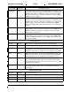
Sundance Technology ST201 byte 3 byte 2 PRELIMINARY draft 2 byte 1 byte 0 Offset 0xe0..
Sundance Technology ST201 PRELIMINARY draft 2 CACHELINESIZE Class....................PCI Configuration Registers, Configuration Base Address ......PCI device configuration header start Address Offset .....0x0c Access Mode .......Read/Write Width ...................8 bits BIT 7..0 BIT NAME CacheLineSize BIT DESCRIPTION The system BIOS writes the system’s cache line size into this register. The adapter uses this to optimize PCI bus master operation (choosing the best memory command, etc.).
Sundance Technology ST201 PRELIMINARY draft 2 CAPPTR Class....................PCI Configuration Registers, Configuration Base Address ......PCI device configuration header start Address Offset .....0x34 Access Mode .......Read Only Width ...................8 bits BIT 7..0 BIT NAME CapPtr BIT DESCRIPTION This is a hard-coded value pointing to the beginning of a chain of registers that describe enhanced functions. The CapPtr register returns 50h, which points to the power management registers.
Sundance Technology ST201 PRELIMINARY draft 2 CLASSCODE Class....................PCI Configuration Registers, Configuration Base Address ......PCI device configuration header start Address Offset .....0x09 Access Mode .......Read Only Width ...................24 bits BIT 23..0 BIT NAME ClassCode BIT DESCRIPTION This register identifies the general function of the PCI device. The ST201 returns 020000h, indicating Ethernet network controller.
Sundance Technology ST201 PRELIMINARY draft 2 CONFIGCOMMAND Class....................PCI Configuration Registers, Configuration Base Address ......PCI device configuration header start Address Offset .....0x04 Access Mode .......Read/Write Width ...................16 bits This register provides control over the adapter’s ability to generate and respond to PCI cycles. When a zero is written to this register, the adapter is logically disconnected from the PCI bus, except for configuration cycles.
Sundance Technology ST201 PRELIMINARY draft 2 CONFIGSTATUS Class....................PCI Configuration Registers, Configuration Base Address ......PCI device configuration header start Address Offset .....0x06 Access Mode .......Read/Write Width ...................16 bits This register is used to record status information for PCI bus events. Read/write bits in the register can only be reset, not set, by writing to this register. Bits are reset by writing a one to that bit position.
Sundance Technology ST201 PRELIMINARY draft 2 DEVICEID Class....................PCI Configuration Registers, Configuration Base Address ......PCI device configuration header start Address Offset .....0x02 Access Mode .......Read Only Width ...................16 bits BIT 15..0 BIT NAME DeviceId BIT DESCRIPTION This register contains the 16-bit device ID for the ST201. It is hardwired to 0201h.
Sundance Technology ST201 PRELIMINARY draft 2 EXPROMBASEADDRESS Class....................PCI Configuration Registers, Configuration Base Address ......PCI device configuration header start Address Offset .....0x30 Access Mode .......Read/Write Width ...................32 bits This read/write register allows the system to define the base address for the adapter’s Expansion ROM. BIT BIT NAME BIT DESCRIPTION 0 AddressDecodeEnable When this bit is cleared, the adapter’s Expansion ROM is disabled.
Sundance Technology ST201 PRELIMINARY draft 2 HEADERTYPE Class....................PCI Configuration Registers, Configuration Base Address ......PCI device configuration header start Address Offset .....0x0e Access Mode .......Read Only Width ...................8 bits BIT 7..0 BIT NAME HeaderType BIT DESCRIPTION This register is hard-wired to 00h, identifying the ST201 as a singlefunction PCI and specifies the configuration register layout.
Sundance Technology ST201 PRELIMINARY draft 2 INTERRUPTLINE Class....................PCI Configuration Registers, Configuration Base Address ......PCI device configuration header start Address Offset .....0x3c Access Mode .......Read/Write Width ...................8 bits BIT 7..0 BIT NAME InterruptLine BIT DESCRIPTION This register is written by the system to communicate to the device driver which interrupt level is being used for the device.
Sundance Technology ST201 PRELIMINARY draft 2 INTERRUPTPIN Class....................PCI Configuration Registers, Configuration Base Address ......PCI device configuration header start Address Offset .....0x3d Access Mode .......Read Only Width ...................8 bits BIT 7..0 BIT NAME InterruptPin BIT DESCRIPTION This register indicates which PCI interrupt pin the adapter will use. ST201-based adapters always use INTAN, so 01h is returned in InterruptPin.
Sundance Technology ST201 PRELIMINARY draft 2 IOBASEADDRESS Class....................PCI Configuration Registers, Configuration Base Address ......PCI device configuration header start Address Offset .....0x10 Access Mode .......Read/Write Width ...................32 bits The host uses this register to define the I/O base address for the adapter. PCI system requires that I/O base addresses be set as if the system used 32-bit I/O addressing.
Sundance Technology ST201 PRELIMINARY draft 2 LATENCYTIMER Class....................PCI Configuration Registers, Configuration Base Address ......PCI device configuration header start Address Offset .....0x0d Access Mode .......Read/Write Width ...................8 bits This register specifies, in units of PCI bus clocks, the value of the latency timer for bus master operations.
Sundance Technology ST201 PRELIMINARY draft 2 MAXLAT Class....................PCI Configuration Registers, Configuration Base Address ......PCI device configuration header start Address Offset .....0x3f Access Mode .......Read Only Width ...................8 bits BIT 7..0 BIT NAME MaxLat BIT DESCRIPTION MaxLat specifies, in 250 ns increments, how often the ST201 requires bus access while operating as a bus master. The value for MaxLat is stored in the ConfigParm word in EEPROM.
Sundance Technology ST201 PRELIMINARY draft 2 MEMBASEADDRESS Class....................PCI Configuration Registers, Configuration Base Address ......PCI device configuration header start Address Offset .....0x14 Access Mode .......Read/Write Width ...................32 bits The host uses this register to define the memory base address for the adapter registers. BIT BIT NAME BIT DESCRIPTION 0 MemBaseAddrInd A value of 1 indicates this register is the memory base address. 2..
Sundance Technology ST201 PRELIMINARY draft 2 MINGNT Class....................PCI Configuration Registers, Configuration Base Address ......PCI device configuration header start Address Offset .....0x3e Access Mode .......Read Only Width ...................8 bits BIT 7..0 BIT NAME MinGnt BIT DESCRIPTION MinGnt specifies, in 250 ns increments, how long a burst period the adapter requires when operating as a bus master. The value for MinGnt is stored in the ConfigParm word in EEPROM.
Sundance Technology ST201 PRELIMINARY draft 2 REVISIONID Class....................PCI Configuration Registers, Configuration Base Address ......PCI device configuration header start Address Offset .....0x08 Access Mode .......Read Only Width ...................8 bits BIT 7..0 BIT NAME RevisionId BIT DESCRIPTION This register provides a revision code for the ST201. The first ST201 will return 00h. Future revisions of the chip will cause this value to be incremented.
Sundance Technology ST201 PRELIMINARY draft 2 SUBSYSTEMID Class....................PCI Configuration Registers, Configuration Base Address ......PCI device configuration header start Address Offset .....0x2e Access Mode .......Read Only Width ...................16 bits BIT 15..0 BIT NAME SubsystemId BIT DESCRIPTION This is the value read from EEPROM word 03h after system reset.
Sundance Technology ST201 PRELIMINARY draft 2 SUBSYSTEMVENDORID Class....................PCI Configuration Registers, Configuration Base Address ......PCI device configuration header start Address Offset .....0x2c Access Mode .......Read Only Width ...................16 bits BIT 15..0 BIT NAME SubsystemVendorId BIT DESCRIPTION This value is read from EEPROM location 02h after system reset.
Sundance Technology ST201 PRELIMINARY draft 2 VENDORID Class....................PCI Configuration Registers, Configuration Base Address ......PCI device configuration header start Address Offset .....0x00 Access Mode .......Read Only Width ...................16 bits BIT 15..0 BIT NAME VendorId BIT DESCRIPTION This register contains the unique 16-bit manufacturer’s ID as allocated by the PCI SIG. Sundance’s manufacturer ID is hard-wired to 0x13f0.
Sundance Technology ST201 PRELIMINARY draft 2 CAPID Class....................PCI Configuration Registers, Power Management Base Address ......PCI device configuration header start Address Offset .....0x50 Access Mode .......Read Only Width ...................8 bits BIT 7..0 BIT NAME CapId BIT DESCRIPTION This register indicates the type of capability data structure. It returns 01h to indicate a PCI Power Management structure.
Sundance Technology ST201 PRELIMINARY draft 2 NEXTITEMPTR Class....................PCI Configuration Registers, Power Management Base Address ......PCI device configuration header start Address Offset .....0x51 Access Mode .......Read Only Width ...................8 bits BIT 7..0 BIT NAME NextItemPtr BIT DESCRIPTION This register points to the next capability data structure in the capabilities list. It returns 00h to indicate that there are no further data structures.
Sundance Technology ST201 PRELIMINARY draft 2 POWERMGMTCAP Class....................PCI Configuration Registers, Power Management Base Address ......PCI device configuration header start Address Offset .....0x52 Access Mode .......Read Only Width ...................16 bits This register provides information about the adapter’s power management capabilities. The reset default is 7601h, but several bits are loaded from EEPROM shortly after reset. BIT BIT NAME BIT DESCRIPTION 2..
Sundance Technology ST201 PRELIMINARY draft 2 POWERMGMTCTRL Class....................PCI Configuration Registers, Power Management Base Address ......PCI device configuration header start Address Offset .....0x54 Access Mode .......Read/Write Width ...................16 bits This register allows control over the power state and the power management interrupts. BIT 1..0 BIT NAME PowerState BIT DESCRIPTION This read/write field is used to determine or set the ST201’s power state.
Sundance Technology ST201 PRELIMINARY draft 2 EEPROM DATA FORMAT Figure 13 summarizes the layout of the EEPROM.
Sundance Technology ST201 PRELIMINARY draft 2 CONFIGPARM Class....................EEPROM Data Format Base Address ......0x00, address written to EepromCtrl register Address Offset .....0x00 Access Mode .......Read Only Width ...................16 bits This is loaded into the ST201 and controls various hardware functions related to PCI bus operation. BIT BIT NAME BIT DESCRIPTION 0 FastBackToBack Determines the value for the FastBackToBack bit in the ConfigStatus register.
Sundance Technology ST201 PRELIMINARY draft 2 STATIONADDRESS Class....................EEPROM Data Format Base Address ......0x00, address written to EepromCtrl register Address Offset .....0x10, 0x12, 0x14 Access Mode .......Read Only Width ...................48 bits This is the field to be programmed into the StationAddress register. OEM customers may choose to program this field with a different value. BIT BIT NAME BIT DESCRIPTION 15..
Sundance Technology ST201 PRELIMINARY draft 2 ASICCTRL Class....................EEPROM Data Format Base Address ......0x00, address written to EepromCtrl register Address Offset .....0x02 Access Mode .......Read Only Width ...................16 bits This word supplies the value for the least significant byte of the AsicCtrl I/O Register. Bit[15] is loaded into WakePolarity of the WakeEvent I/O Register.
Sundance Technology BIT ST201 BIT NAME PRELIMINARY draft 2 BIT DESCRIPTION 14..8 Reserved Reserved for future use. Should be set to 0. 15 ResetPolarity Setting this read/write bit will cause the RSTOUT pin to be asserted in the HIGH state (default after RESET).
Sundance Technology ST201 SUBSYSTEMVENDORID Address Offset .... 0x04 Class....................EEPROM Data Format Base Address ......0x00, address written EepromCtrl register BIT 15..0 Access Mode....... Read Only to Width ................... 16 bits BIT NAME SubsystemVendorId PRELIMINARY draft 2 BIT DESCRIPTION This is the two-byte subsystem vendor ID. Since in this case the subsystem is an adapter, customers needs to use their PCI vendor ID.
Sundance Technology ST201 SUBSYSTEMID Address Offset .... 0x06 Class....................EEPROM Data Format Base Address ......0x00, address written EepromCtrl register BIT 15..0 Access Mode....... Read Only to Width ................... 16 bits BIT NAME SubsystemId PRELIMINARY draft 2 BIT DESCRIPTION This is the two-byte subsystem ID for the adapters, the same code as the DeviceId is used.
Sundance Technology ST201 PRELIMINARY draft 2 ABSOLUTE MAXIMUM RATINGS OPERATING RANGES Storage Temperature ..................-65ºC to +150ºC Commercial Devices Ambient Temperature ....................-65ºC to +70ºC Temperature (TA) ............................. 0ºC to +70ºC Supply Voltage ...............................-0.3V to +6.0V Supply Voltages (V CC) ............................+5V ±5% Input voltages..........................................
Sundance Technology ST201 PRELIMINARY draft 2 DC CHARACTERISTICS DC characteristics are defined over commercial operating ranges unless specified otherwise. PARAMETER SYMBOL PARAMETER DESCRIPTION TEST CONDITIONS MIN MAX UNIT PIN TYPE IT (TTL, PCI INPUT BUFFER) VIH Input high voltage 2 V VIL Input low voltage 0.8 V IIN Input leakage current 10 µA VIN = VDD/VSS -10 PIN TYPE ITU (TTL, PCI INPUT BUFFER WITH PULL UP) VIH Input high voltage 2 V VIL Input low voltage 0.
Sundance Technology PARAMETER SYMBOL ST201 PARAMETER DESCRIPTION PRELIMINARY draft 2 TEST CONDITIONS MIN MAX UNIT 0.4 V 10 µA 0.
Sundance Technology ST201 PIN TYPE PRELIMINARY draft 2 PINS MISC INTERFACE ITU/OT4 GPIO0, GPIO1 OT4 RSTOUT OD8 LEDPWRN, LEDLNKN, LEDDPLXN, LEDSPDN OC4 CLK25 OSCI X25I OSCOH1 X25O TABLE 5: Pin Type Assignment 138
Sundance Technology ST201 PRELIMINARY draft 2 SWITCHING CHARACTERISTICS PARAMETER SYMBOL PARAMETER DESCRIPTION TEST CONDITIONS MIN MAX UNIT PCI INTERFACE Trc RSTN cycle 300 - - Tcc PCICLK cycle 30 - - Tch PCICLK high 11 - - Tcl PCICLK low 11 - - Trv PCICLK rise to bused signal valid 2 11 - Trvp PCICLK rise to REQN, GNTN valid 2 12 - Trzo PCICLK rise to signal on 2 - - Troz PCICLK rise to signal off - 28 - Tsu bused signal setup wrt PCICLK rise 7 - - Tsup
Sundance Technology PARAMETER SYMBOL ST201 PARAMETER DESCRIPTION TEST CONDITIONS PRELIMINARY draft 2 MIN MAX UNIT Twh EWEN write cycle high 100 - - Twl EWEN write cycle low 90 - - EEPROM INTERFACE Tskc EESK cycle 1us - - Tskh EESK high 250 - - Tskl EESK low 250 - - Tcs EECS low 250 - - Tpd EEDI valid wrt EESK rise 100 - - Tcsk EECS setup wrt EESK rise 50 - - Tcsh EECS hold wrt EESK fall 0 - - Tdos EEDO setup wrt EESK rise 70 500 - Tdoh EEDO hold wrt
Sundance Technology PARAMETER SYMBOL ST201 PARAMETER DESCRIPTION TEST CONDITIONS PRELIMINARY draft 2 MIN MAX UNIT MII INTERFACE - MANAGEMENT Tcc MDC cycle 400 - - Tch MDC high 160 - - Tcl MDC low 160 - - Tsu MDIO setup wrt MDC rise 10 - - Thd MDIO hold wrt MDC rise 10 - - Trv MDC rise to MDIO valid - 20 - MISC INTERFACE Tcc CLK25 cycle - - 40 Tch CLK25 high 16 24 - Tcl CLK25 low 16 24 - TABLE 6: Switching Characteristics 141
Sundance Technology ST201 PRELIMINARY draft 2 trc RSTN tcl tcc PCICLK trv tsu ST201 BUSSED SIGNALS trvp tsup2 trvp tsup1 REQN GNTN thd trzo ANY SIGNAL trstoff troz ANY SIGNAL tabc FIGURE 14: PCI Switching Characteristics Read Load EOEN ST201 tos twl toh EWEN tas tah twh EA[15..0] todv tadv tdvz tds tdh ED[7..
Sundance Technology ST201 PRELIMINARY draft 2 tcsh tcs EECS ST201 tcsk tskl tskc tskh EESK tpd EEDI A7 A0 tdos EEDO tdoh D15 FIGURE 16: EEPROM Switching Characteristics 143 D0
Sundance Technology ST201 PRELIMINARY draft 2 Transmit TXD[3..0] trv trh trv trh TXEN tcl tcc tch tcc tch tcc tch TXCLK Receive ST201 RXD[3..
Sundance Technology ST201 PRELIMINARY draft 2 PHYSICAL DIMENSIONS Copyright Sundance Technology, Inc., 1998. The information contained in this data sheet is subject to change without notice. Sundance Technology assumes no responsibility for the use of any circuitry other than circuitry embodied in a Sundance Technology product. Nor does it convey or imply any license under patent or other rights.