
Application Guide


0.076mm
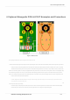
Figure 2: Schematic diagram of the coplanar waveguide structure
0.1623mm
Sunivision Technology Development Co.,Ltd
6 / 9
The main factors affecting the characteristic impedance of coplanar waveguides are the dielectric constant of the substrate (usually
0.1188mm
Line width W
It is recommended to use the coplanar waveguide microwave transmission form, and the characteristic impedance is 50 ohms, as shown in Figure 2.
Ground clearance S
0.24mm 0.2mm
0.2mm
Table 1: 50 ohm coplanar waveguide line width and recommended distance to ground corresponding to the distance between different signal layers and reference ground
RF LAYOUT Application Guide
Distance H between signal layer and reference ground
0.15mm
4.2ÿ4.6, take here
4.4), the distance between the signal layer and the reference ground H, the line width W, the ground clearance S, and the copper thickness T. Table 1 lists the distance H between different signal layers and the reference ground
0.15mm
0.1mm
When the thickness of copper skin is T=0.035mm, the line width W corresponding to the characteristic impedance of 50 ohms and the recommended value of the ground clearance S:
3 50 Ohm Characteristic Impedance Coplanar Waveguide Structure Design