
User Guide

2-10
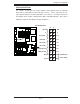
X7DVL-3/X7DVL-i User's Manual
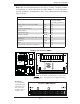
LAN1
®
S
UPER X7DVL-3
FP Control
Fan3
IDE1
Fan4
SATA3
SATA5
PCI 33 MHz
Battery
GLAN
CTRLR
North Bridge
COM1
ATX PWR
8-Pin
PWR
24-Pin
CPU2
South
Bridge
Fan1
SATA2
SATA4
SATA1
SATA0
Slot1
PCI-X 133 MHz
JPL2
Slot5
DIMM 1A (Bank 1)
DIMM 1B (Bank 1)
DIMM 1C (Bank 1)
DIMM 2A (Bank 2)
DIMM 2B (Bank 2)
DIMM 2C (Bank 2)
JBT1
JCOM2
KB/
Mouse
USB 0/1
5000V
LAN2
Fan5
Fan6
JPWF
JAR
PWR
I
2
C
VGA
Slot6
PCI-X 133 MHz
PCI-E x8
JPG1
JWD
Printer
JPL1
JI
2
C1
JI
2
C2
JWOR
JWOL
Fan2
CPU1
LE2
LE3
LE1
LE5
LE4
SAS0
USB2/3
JPF
Buzzer
ESB2
VGA
CTRLR
T-SGPIO1
JL1
D31
I-Button
SIMLP
Floppy
USB4/5
T-SGPIO0
JD1
BIOS
SAS1
SAS2
SAS3
SAS4
SAS5
SAS6
SAS7
CPU VRM
CPU VRM
Graphics
Memory
S I/O
LSI SAS
Controller
JF1
3-SGPIO1
3-SGPIO0
JPA2
JPA1
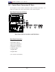
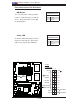
Power LED
The Power LED connection is located
on pins 15 and 16 of JF1. Refer to the
table on the right for pin defi nitions.
NMI Button
The non-maskable interrupt button
header is located on pins 19 and 20
of JF1. Refer to the table on the right
for pin defi nitions.
Power Button
OH/Fan Fail LED
1
NIC1 LED
Reset Button
2
HDD LED
Power LED
Reset
PWR
Vcc
Vcc
Vcc
Vcc
Ground
Ground
1920
Vcc
X
Ground
NMI
X
Vcc
PWR Fail LED
NIC2 LED
NMI Button
Pin Defi nitions (JF1)
Pin# Defi nition
19 Control
20 Ground
Power LED
Pin Defi nitions (JF1)
Pin# Defi nition
15 +5V
16 Ground
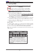
Front Control Panel Pin Defi nitions
A. NMI
B. PWR LED
A
B