
Specifications
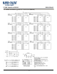

512MB Unbuffered DIMM DDR SDRAM
Products and Specifications discussed herein are subject to change without notice © 2006 Super Talent Tech., Corporation.
2
1.0 Feature
• V
DD
: 2.5V ± 0.2V, V
DDQ
: 2.5V ± 0.2V for DDR333
• V
DD
: 2.6V ± 0.1V, V
DDQ
: 2.6V ± 0.2V for DDR400
• Double-data-rate architecture; two data transfers per clock cycle
• Bidirectional data strobe [DQ] x8)
• Differential clock inputs(CK and CK)
• DLL aligns DQ and DQS transition with CK transition
• Programmable Read latency : DDR333(2.5 Clock), DDR400(3 Clock)
• Programmable Burst length (2, 4, 8)
• Programmable Burst type (sequential & interleave)
• Edge aligned data output, center aligned data input
• Auto & Self refresh, 7.8us refresh interval(8K/64ms refresh)
• Serial presence detect with EEPROM
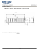
• PCB : Height 1,250 (mil) & single (512MB), double (512MB) sided
• SSTL_2 Interface
• 66pin TSOP II package
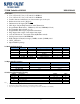
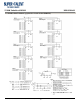
2.0 Ordering Information
Part number Density Organization Component composition No. of rank Height
x64 Non ECC
D32PB12C25 512MB 64x64 32mx8 TSOP II 2 1.25”
D32PA512N 512MB 64x64 64Mx8 TSOP II 1 1.25”
x72 ECC
512MB 64x72 32mx8 TSOP II 2
512MB 64x72 64Mx8 TSOP II 1
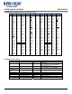
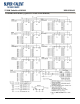
3.0 Operating Frequencies
CC(DDR400@CL=3) B3(DDR333@CL=2.5)
Speed @CL2 133MHz
Speed @CL2.5 166MHz 166MHz
Speed @CL3 200Mhz
CL-tRCD-tRP 3-3-3 2.5-3-3
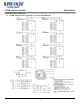
4.0 Absolute Maximum DC Rating
Symbol Parameter Rating Units
V
in,
Vout Voltage on any pin relative to V
SS
-0.5 ~ 3.6 V
V
DD
, V
DDQ
Voltage on V
DD
& Vddq supply relative to Vss
-1.0 ~ 3.6 V
Ios Short circuit current 50 mA
Pd Power dissipation 1.5 * #of component w
T
STG
Storage Temperature 55 ~ + 150 °C
Note:
• Permanent device damage may occur if ABSOLUTE MAXIMUM RATINGS are exceeded.
• Functional operation should be restricted to recommended operating condition.
• Exposure to higher than recommended voltage for extended periods of time could affect device reliability.