
Specifications

512MB Unbuffered DIMM DDR SDRAM
Products and Specifications discussed herein are subject to change without notice © 2006 Super Talent Tech., Corporation.
9
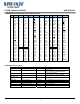
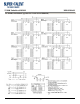
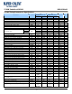
11.0 AC Timing Parameters & Specifications
CC
(DDR400@CL=3.0)
B3
(DDR333@CL=2.5)
Parameter Symbol
Min Max Min Max
Unit Note
Row cycle time tRC 55 60 ns
Refresh row cycle time tRFC 70 72 ns
Row active time tRAS 40 70K 42 70K ns
RAS to CAS delay tRCD 15 18 ns
Row precharge time tRP 15 18 ns
Row active to Row active delay tRRD 10 12 ns
Write recovery time tWR 15 15 ns
Last data in to Read command tWTR 2 1 tCK
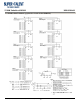
CL=2.0 - - 7.5 12 ns
CL=2.5 6 12 6 12 ns
Clock cycle time
CL=3.0
tCK
5 10 - -
Clock high level width tCH 0.45 0.55 0.45 0.55 tCK
Clock low level width tCL 0.45 0.55 0.45 0.55 tCK
DQS-out access time from CK/CK tDQSCK -0.55 +0.55 -0.6 +0.6 ns
Output data access time from CK/CK tAC -0.65 +0.65 -0.7 +0.7 ns
Data strobe edge to output data edge tDQSQ - +0.4 - +0.45 ns
Read Preamble tRPRE 0.9 1.1 0.9 1.1 tCK
Read Postamble tRPST 0.4 0.6 0.4 0.6 tCK
CK to valid DQS-in tDQSS 0.72 1.28 0.75 1.25 tCK
DQS-in setup time tWPRES 0 0 ns
DQS-in hold time tWPRE 0.25 0.25 tCK
DQS falling edge to CK rising-setup time tDSS 0.2 0.2 tCK
DQS falling edge from CK rising-setup time tDSH 0.2 0.2 tCK
DQS-in high level width tDQSH 0.35 0.35 tCK
DQS-in low level width tDQSL 0.35 0.35 tCK
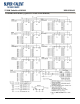
Address and Control input setup time (fast) tIS 0.6 0.75 ns
Address and Control input hold time (fast) tIH 0.6 0.75 ns
Address and Control input setup time (slow) tIS 0.7 0.8 ns
Address and Control input hold time (slow) tIH 0.7 0.8 ns
Data-out high impedance time from CK/CK tHZ -0.65 +0.65 -0.7 +0.7 ns
Data-out low impedance time from CK/CK tLZ -0.65 +0.65 -0.7 +0.7 ns
Mode register set cycle time tMRD 10 12 ns
DQ & DM setup time to DQS tDS 0.4 0.45 ns
DQ & DM hold time to DQS tDH 0.4 0.45 ns
Control & Address input pulse width tIPW 2.2 2.2 ns
DQ & DM input pulse width tDIPW 1.75 1.75 ns
Exit self refresh to non-Read command tXSNR 75 75 ns
Exit self refresh to Read command tXSRD 200 200 tCK
Refresh interval time tREFI 7.8 7.8 ns
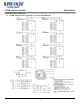
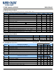
Output DQS valid window
tQH THP-
tQHS
-
THP-
tQHS
-
ns
Clock half period
tHP TCLmin
or tCHmin
-
TCLmin
or tCHmin
-
ns
Data hold skew factor tQHS 0.5 0.55 ns
DQS write postamble time tWPST 0.4 0.6 0.4 0.6 tCK
Active to Read with Auto precharge command tRAP 15 18
Autoprecharge write recovery + Precharged time tDAL (tWR/tCK
) +
(tRP/tCK)
(tWR/tCK
) +
(tRP/tCK)
tCK