
Data Sheet

GENERAL FEATURES:
• Operating voltage: 3V to 5.5V (V
DD - VSS)
• 5V count frequency: 40MHz
• 3V count frequency: 20MHz
• 32-bit counter (CNTR).
• 32-bit data register (DTR) and comparator.
• 32-bit output register (OTR).
• Two 8-bit mode registers (MDR0, MDR1)
for programmable functional modes.
• 8-bit instruction register (IR).
• 8-bit status register (STR).
• Latched Interrupt output on Carry or Borrow or Compare or Index.
• Index driven counter load, output register load or counter reset.
• Internal quadrature clock decoder and filter.
• x1, x2 or x4 mode of quadrature counting.
• Non-quadrature up/down counting.
• Modulo-N, Non-recycle, Range-limit or
Free-running modes of counting
• 8-bit, 16-bit, 24-bit and 32-bit programmable configuration
synchronous (SPI) serial interface
• LS7366R (DIP), LS7366R-S (SOIC), LS7366R-TS (TSSOP)
- See Figure 1 -
SPI/MICROWIRE (Serial Peripheral Interface):
• Standard 4-wire connection: MOSI, MISO, SS/ and SCK.
• Slave mode only.
GENERAL DESCRIPTION:
LS7366R is a 32-bit CMOS counter, with direct interface for quadra-
ture clocks from incremental encoders. It also interfaces with the
index signals from incremental encoders to perform variety of
marker functions.
For communications with microprocessors or microcontrollers, it
provides a 4-wire SPI/MICROWIRE bus.The four standard bus I/Os
are SS/, SCK, MISO and MOSI. The data transfer between a micro-
controller and a slave LS7366R is synchronous. The synchroniza-
tion is done by the SCK clocks supplied by the microcontroller. Each
transmission is organized in blocks of 1 to 5 bytes of data. A trans-
mission cycle is intitiated by a high to low transition of the SS/ input.
The first byte received in a transmission cycle is always an instruc-
tion byte, whereas the second through the fifth bytes are always
interpreted as data bytes. A transmission cycle is terminated with
the low to high transition of the SS/ input. Received bytes are shifted
in at the MOSI input, MSB first, with the leading edges (high transi-
tion) of the SCK clocks. Output data are shifted out on the MISO
output, MSB first, with the trailing edges (low transition) of the SCK
clocks.
32-BIT QUADRATURE COUNTER WITH SERIAL INTERFACE
LSI/CSI
LSI Computer Systems, Inc. 1235 Walt Whitman Road, Melville, NY 11747 (631) 271-0400 FAX (631) 271-0405
LS7366R
U
L
®
A3800
December 2007
7366R-120407-1
Read and write commands cannot be combined.
For example, when the device is shifting out read
data on MISO output, it ignores the MOSI input,
even though the SS/ input is active. SS/ must be
terminated and reasserted before the device will
accept a new command.
The counter can be configured to operate as 1, 2, 3
or 4-byte counter. When configured as an n-byte
counter, the CNTR, DTR and OTR are all config-
ured as n-byte registers, where n = 1, 2, 3 or 4.
The content of the instruction/data identity is
automatically adjusted to match the n-byte configu-
ration. For example, if the counter is configured as a
2-byte counter, the instruction “write to DTR”
expects 2 data bytes following the instruction byte.
If the counter is configured as a 3-byte counter, the
same instruction will expect 3 bytes of data follow-
ing the instruction byte.
Following the transfer of the appropriate number of
bytes any further attempt of data transfer is ignored
until a new instruction cycle is started by switching
the SS/ input to high and then low.
The counter can be programmed to operate in a
number of different modes, with the operating
characteristics being written into the two mode
registers MDR0 and MDR1. Hardware I/Os are
provided for event driven operations, such as
processor interrupt and index related functions.
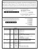
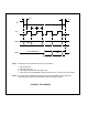
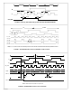
1
2
3
4
5
6
7
8
9
10
11
12
13
V
SS
14
V
DD
B
A
INDEX/
LFLAG/
SS/
SCK
LS7366R
MISO
MOSI
f
CKi
fCKO
CNT_EN
DFLAG/
FIGURE 1
LSI
PIN ASSIGNMENT
TOP VIEW