H8QC8 H8QC8+ H8QCE H8QCE+ USER’S MANUAL Revision 1.
The information in this User’s Manual has been carefully reviewed and is believed to be accurate. The vendor assumes no responsibility for any inaccuracies that may be contained in this document, makes no commitment to update or to keep current the information in this manual, or to notify any person or organization of the updates. The manufacturer reserves the right to make changes to the product described in this manual at any time and without notice.
Preface Preface About This Manual This manual is written for system integrators, PC technicians and knowledgeable PC users. It provides information for the installation and use of the H8QC8/H8QC8+/H8QCE/H8QCE+ serverboard. The H8QC8(+)/H8QCE(+) is based on the nVidia® nForce Pro 2200 (CK804) and the AMD 8132 chipset and supports four AMD Opteron 800 series type processors in 940-pin microPGA ZIF sockets and up to 64 GB of DDR266 or 32 GB of DDR400/333 registered ECC SDRAM.
H8QC8(+)/H8QCE(+) User’s Manual Table of Contents Preface About This Manual ...................................................................................................... iii Manual Organization ................................................................................................... iii Chapter 1: Introduction 1-1 Overview ......................................................................................................... 1-1 Checklist .............................................
Table of Contents Reset Button ............................................................................................ 2-9 Power Button ............................................................................................ 2-9 Universal Serial Bus Ports (USB0/1) ....................................................... 2-9 Extra USB Headers ................................................................................ 2-10 Serial Ports ............................................................
H8QC8(+)/H8QCE(+) User’s Manual 2-10 Enabling SATA RAID .................................................................................... 2-23 Chapter 3: Troubleshooting 3-1 Troubleshooting Procedures ........................................................................... 3-1 Before Power On ..................................................................................... 3-1 No Power .................................................................................................
Chapter 1: Introduction Chapter 1 Introduction 1-1 Overview Checklist Congratulations on purchasing your computer serverboard from an acknowledged leader in the industry. Our boards are designed with the utmost attention to detail to provide you with the highest standards in quality and performance. Please check that the following items have all been included with your serverboard. If anything listed here is damaged or missing, contact your retailer.
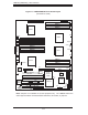
H8QC8(+)/H8QCE(+) User’s Manual Figure 1-1. H8QC8/H8QCE Image Note: The H8QC8 is shown. The H8QCE shares the same layout but does not include SCSI controllers, connectors, or jumpers.
Chapter 1: Introduction Figure 1-2. H8QC8+/H8QCE+ Image Note: The H8QC8+ is shown. The H8QCE+ shares the same layout but does not include SCSI controllers, connectors, or jumpers.
H8QC8(+)/H8QCE(+) User’s Manual Figure 1-3.
Chapter 1: Introduction H8QC8/H8QCE Quick Reference Jumpers Description Default Setting J3P 3rd Power Fail Detect Open (Disabled) JBT1 JI2C1/JI2C2 CMOS Clear I2C to PCI-X # 1 & 2 Slots See Section 2-7 Both Pins 1-2 (Enabled) JI2C3/JI2C4 I2C to PCI-X # 3 & 4 Slots Both Pins 1-2 (Enabled) JP1/JP2 Compact Flash Drive Select Both Closed (Master) JPA1* JPA2/JPA3* SCSI Enable/Disable SCSI CH A/B Termination Pins 1-2 (Enabled) Both Open (Enabled) JPG1 VGA Enable/Disable Pins 1-2 (Enabled) JPL
H8QC8(+)/H8QCE(+) User’s Manual Figure 1-4.
Chapter 1: Introduction H8QC8+/H8QCE+ Quick Reference Jumpers Description Default Setting J3P 3rd Power Fail Detect Open (Disabled) JBT1 CMOS Clear See Section 2-7 JP1/JP2 JPA1* Compact Flash Drive Select SCSI Enable/Disable Both Closed (Master) Pins 1-2 (Enabled) JPA2/JPA3* SCSI CH A/B Termination Both Open (Enabled) JPG1 VGA Enable/Disable Pins 1-2 (Enabled) JPL1 GLAN Enable/Disable Pins 1-2 (Enabled) JWD Watch Dog Pins 1-2 (Reset) Connectors Description COM1, COM2 FAN 1-9 Flopp
H8QC8(+)/H8QCE(+) User’s Manual Serverboard Features CPU • Four AMD Opteron 800 series 64-bit processors in 940-pin microPGA ZIF sockets (the use of less than four CPUs is not recommended) Memory • Sixteen dual/single channel DIMM slots (four per CPU) supporting up to 64 GB of DDR333/266 registered ECC or up to 32 GB of DDR400 registered ECC SDRAM Note: Refer to Section 2-4 before installing.
Chapter 1: Introduction ACPI Features • Microsoft OnNow • Slow blinking LED for suspend state indicator • BIOS support for USB keyboard • Main switch override mechanism • Internal/external modem ring-on Onboard I/O • On-chip SATA controller supporting four (4) SATA ports (RAID 0, 1, 0+1) • Adaptec AIC-7902 controller for dual-channel Ultra320 SCSI (H8QC8 and H8QC8+ only) • Two (2) UltraDMA133/100 IDE ports • One (1) floppy port interface (up to 2.
H8QC8(+)/H8QCE(+) User’s Manual DDR400/333/266 DDR400/333/266 DIMM 2B DIMM 2A DIMM 1B DIMM 1A TM AMD Opteron CPU #3 128-bit data+ 16-bit ECC DIMM 2B DIMM 2A DIMM 1B DIMM 1A AMD Opteron CPU #2 16 x 16 HT link 16 x 16 HT link (1 GHz) (1 GHz) AMD OpteronTM CPU #4 DIMM 2B DIMM 2A DIMM 1B DIMM 1A TM 128-bit data + 16-bit ECC DIMM 2B DIMM 2A DIMM 1B DIMM 1A AMD OpteronTM CPU #1 16 x 16 HT link (1 GHz) Slot #1: PCI-X 100 MHz Slot #5: PCI-E x8 Slot #2: PCI-X 100 MHz PCI-E Dual SCSI Channels
Chapter 1: Introduction 1-2 Chipset Overview The H8QC8(+)/H8QCE(+) serverboard is based on the nVidia nForce Pro 2200 (CK804) and AMD 8132 chipset components. The 2200 functions as a Media and Communications Processors (MCP) while the 8132 acts as the PCI hub. Both hubs connect to the processors and through them to system memory (the memory controllers are integrated directly into the AMD Opteron processors).
H8QC8(+)/H8QCE(+) User’s Manual 1-3 PC Health Monitoring This section describes the PC health monitoring features of the H8QC8(+)/ H8QCE(+). The serverboard has an onboard System Hardware Monitor chip that supports PC health monitoring. Onboard Voltage Monitors for CPU cores, Hyper Transport (1.2V), two memory banks (2.5V), nVidia 2200 chipset (1.5V) The onboard voltage monitor will scan these voltages continuously.
Chapter 1: Introduction 1-4 Power Configuration Settings This section describes the features of your serverboard that deal with power and power settings. Microsoft OnNow The OnNow design initiative is a comprehensive, system-wide approach to system and device power control. OnNow is a term for a PC that is always on but appears to be off and responds immediately to user or other requests.
H8QC8(+)/H8QCE(+) User’s Manual Wake-On-Ring Header (JWOR) Wake-up events can be triggered by a device such as the external modem ringing when the system is in the SoftOff state. Note that external modem ring-on can only be used with an ATX 2.01 (or above) compliant power supply. Recovery from AC Power Loss BIOS provides a setting for you to determine how the system will respond when AC power is lost and then restored to the system.
Chapter 1: Introduction 1-6 Super I/O The disk drive adapter functions of the Super I/O chip include a floppy disk drive controller that is compatible with industry standard 82077/765, a data separator, write pre-compensation circuitry, decode logic, data rate selection, a clock generator, drive interface control logic and interrupt and DMA logic. The wide range of functions integrated onto the Super I/O greatly reduces the number of components required for interfacing with floppy disk drives.
H8QC8(+)/H8QCE(+) User’s Manual Contacting Supermicro Headquarters Address: Tel: Fax: Email: Web Site: SuperMicro Computer, Inc. 980 Rock Ave. San Jose, CA 95131 U.S.A. +1 (408) 503-8000 +1 (408) 503-8008 marketing@supermicro.com (General Information) support@supermicro.com (Technical Support) www.supermicro.com Europe Address: Tel: Fax: Email: SuperMicro Computer B.V. Het Sterrenbeeld 28, 5215 ML 's-Hertogenbosch, The Netherlands +31 (0) 73-6400390 +31 (0) 73-6416525 sales@supermicro.
Chapter 2: Installation Chapter 2 Installation 2-1 Static-Sensitive Devices Electric Static Discharge (ESD) can damage electronic components. To prevent damage to your system board, it is important to handle it very carefully. The following measures are generally sufficient to protect your equipment from ESD. Precautions • Use a grounded wrist strap designed to prevent static discharge. • Touch a grounded metal object before removing the board from the antistatic bag.
H8QC8(+)/H8QCE(+) User's Manual 2-2 Processor and Heatsink Installation Exercise extreme caution when handling and installing the proces- ! sor. Always connect the power cord last and always remove it before adding, removing or changing any hardware components. Installing the CPU Backplates Four CPU backplates (BKT-0004) are included in the retail box. The backplates prevent the CPU area of the serverboard from bending and provide a base for attaching the heatsink retention modules.
Chapter 2: Installation 4. With the CPU inserted into the socket, inspect the four corners of the CPU to make sure that it is properly installed and flush with the socket. 5. Gently press the CPU socket lever down until it locks in the plastic tab. Repeat these steps to install CPUs into the other three CPU sockets. Installing the Heatsink Retention Modules Four heatsink retention modules (BKT-0005) and eight screws are included in the retail box.
H8QC8(+)/H8QCE(+) User's Manual 2-3 Mounting the Serverboard into a Chassis All serverboards and motherboards have standard mounting holes to fit different types of chassis. Make sure that the locations of all the mounting holes for both the serverboard and the chassis match. Although a chassis may have both plastic and metal mounting fasteners, metal ones are highly recommended because they ground the serverboard to the chassis. Make sure that the metal standoffs click in or are screwed in tightly. 1.
Chapter 2: Installation Support The H8QC8(+)/H8QCE(+) supports single or dual-channel, registered ECC DDR400/333/266 SDRAM. Both interleaved and non-interleaved memory are supported, so you may populate any number of DIMM slots (see note on previous page). Populating two adjacent slots at a time with memory modules of the same size and type will result in interleaved (128-bit) memory, which is faster than non-interleaved (64-bit) memory.
H8QC8(+)/H8QCE(+) User's Manual 2-5 I/O Port and Control Panel Connections The I/O ports are color coded in conformance with the PC99 specification to make setting up your system easier. See Figure 2-3 below for the colors and locations of the various I/O ports. Figure 2-3. I/O Port Locations and Definitions Front Control Panel JF1 contains header pins for various front control panel connectors. See Figure 2-4 for the pin definitions of the various connectors. Refer to Section 2-6 for details. Figure 2-4.
Chapter 2: Installation 2-6 Connecting Cables ATX Power 24-pin Connector Pin Definitions (J1B1) ATX Power Connector Pin# Definition 13 +3.3V 1 +3.3V 14 -12V 2 +3.3V 15 COM 3 COM 16 PS_ON 4 +5V tions of the ATX 24-pin power connec- 17 COM 5 COM tor. This connection supplies power to 18 COM 6 +5V the chipset, fans and memory. 19 COM 7 COM 20 Res (NC) 8 PWR_OK 21 +5V 9 5VSB 22 +5V 10 +12V 23 +5V 11 +12V 24 COM 12 +3.
H8QC8(+)/H8QCE(+) User's Manual HDD LED HDD LED Pin Definitions (JF1) The HDD (IDE Hard Disk Drive) LED connection is located on pins 13 and 14 of JF1. Attach the IDE hard drive LED cable to display disk activity. Pin# Definition 13 Vcc 14 HD Active Refer to the table on the right for pin definitions. NIC1 LED NIC1 LED Pin Definitions (JF1) The NIC1 (Network Interface Controller) LED connection is located on pins 11 and 12 of JF1. Attach the NIC1 LED cable to display network activity.
Chapter 2: Installation Power Fail LED Power Fail LED Pin Definitions (JF1) The Power Fail LED connection is located on pins 5 and 6 of JF1. Refer to the table on the right for pin definitions. This feature is only available Pin# Definition 5 Vcc 6 Control for systems with redundant power supplies. Reset Button Reset Button Pin Definitions (JF1) The Reset Button connection is located on pins 3 and 4 of JF1. Attach it to the hardware reset switch on the computer case.
H8QC8(+)/H8QCE(+) User's Manual Extra USB Headers Extra Universal Serial Bus Headers Pin Definitions (USB2/3) Tw o a d d i t i o n a l U S B 2 . 0 h e a d ers (USB2/3) are included on the USB2 Pin # Definition USB3 Pin # Definition 1 +5V 1 +5V 2 PO- 2 PO- A USB cable (not included) is needed 3 PO+ 3 PO+ for the connection. See the table on 4 Ground 4 Ground the right for pin definitions. 5 Key 5 No connection serverboard. These may be connected to provide front side access.
Chapter 2: Installation Speaker Connector Pin Definitions (JF2) Power LED/Keylock/Speaker Pin# Definition On the JF2 header, pins 2, 4 and 6 1 Red wire, speaker data are for the power LED, pins 8 and 10 3 NC are for the keylock and pins 1, 3, 5 and 7 are for the speaker (there is no 5 Buzzer signal 7 Speaker data pin 9). See the tables on the right for pin definitions and below right for pin locations Note: The speaker connector pins are for use with an external speaker.
H8QC8(+)/H8QCE(+) User's Manual Wake-On-LAN Wake-On-LAN Pin Definitions (JWOL) The Wake-On-LAN header is designated JWOL. See the table on the Pin# Definition right for pin definitions. You must have a LAN card with a Wake-On-LAN 1 +5V Standby 2 Ground 3 Wake-up connector and cable to use the WakeOn-LAN feature. Wake-On-Ring The Wake-On-Ring header is designated JWOR. This function allows your computer to receive and "wakeup" by an incoming call to the modem when in suspend state.
Chapter 2: Installation I2C Header for Power Supply Pin Definitions (J16) I2C Header for Power Supply The I2C header at J16 may be used Pin# Definition to monitor the power supply. See the 1 Clock table on the right for pin definitions. 2 Data 3 PWR Fail 4 Gnd 5 +3.3V SMBus Header Pin Definitions (JSMB) SMBus Header The JSMB header is provided for System Management Bus connection. See the table on the right for pin definitions.
H8QC8(+)/H8QCE(+) User's Manual 2-7 Jumper Settings Explanation of Jumpers To modify the operation of the serverboard, jumpers can be used to 3 2 1 3 2 1 Connector Pins choose between optional settings. Jumpers create shorts between two pins to change the function of the Jumper connector. Pin 1 is identified with a square solder pad on the printed circuit board. See the diagram at right for an example of jumping pins 1 and 2. Refer to the serverboard layout page for jumper locations.
Chapter 2: Installation I2C to PCI-X Slots #1,2 Enable/Disable (H8QC8/ H8QCE only) I2C to PCI# 1,2 Enable/Disable Jumper Settings (JI2C1/2) 2 The JI C1/2 pair of jumpers allows you to connect the System Management Bus to PCI-X slots #1 and 2. The default setting is open (disabled) for Jumper Setting Closed Enabled both jumpers to enable the connec- Open Disabled Definition tion. Both connectors must be set the same (JI2C1 is for data and JI2C2 is for the clock).
H8QC8(+)/H8QCE(+) User's Manual SCSI Termination Enable/ Disable (H8QC8/H8QC8+ only) SCSI Term. Enable/Disable Jumper Settings (JPA2/JPA3) Jumpers JPA2 and JPA3 are used to enable or disable termination for SCSI Jumper Setting Definition Open Enabled Closed Disabled channels A and B, respectively. The default setting is open to enable termination. See the table on right for jumper settings.
Chapter 2: Installation Watch Dog Enable/Disable JWD controls the Watch Dog function. Watch Dog is a system monitor that Watch Dog Jumper Settings (JWD) can reboot the system when a software application hangs. Pins 1-2 will cause Jumper Setting Definition Pins 1-2 Reset WD to reset the system if an applica- Pins 2-3 Disabled tion has frozen. Pins 2-3 will disable the Watch Dog feature. See the table on the right for jumper settings.
H8QC8(+)/H8QCE(+) User's Manual PCI-X Slot Frequency Select (H8QC8/H8QCE only) PCI-X Slot #3/#4 Frequency Select Jumper Settings (JPXB1) Jumper JPXB1 is are used to set the speed of PCI-X slots #3 and #4, Jumper Setting respectively. The recommended (default) setting is open for Auto. See the Pins 1-2 66 MHz PCI-X Pins 2-3 66 MHz PCI Open Auto table on the right for jumper settings.
Chapter 2: Installation 2-9 Floppy, IDE, Parallel Port, SCSI and SATA Drive Connections Use the following information to connect the floppy and hard disk drive cables. The floppy disk drive cable has seven twisted wires. A red mark on a wire typically designates the location of pin 1. A single floppy disk drive ribbon cable has 34 wires and two connectors to provide for two floppy disk drives.
H8QC8(+)/H8QCE(+) User's Manual IDE Connectors IDE Drive Connectors Pin Definitions (IDE#1/IDE#2) There are no jumpers to config- Pin# Definition ure the onboard IDE#1 and #2 1 Reset IDE 2 Ground connectors. See the table on the right for pin definitions.
Chapter 2: Installation Parallel Port Connector Parallel Port Connector Pin Definitions Pin# Definition The parallel (printer) port is 1 Strobe- 2 Auto Feed- located on the I/O backplane. 3 Data Bit 0 4 Error- See the table on the right for pin definitions.
H8QC8(+)/H8QCE(+) User's Manual SCSI Connectors (H8QC8/H8QC8+ only) Ultra320 SCSI Drive Connectors Pin Definitions (JA1/JB1) Pin# Definition Pin # Definition Refer to the table at right for 1 +DB (12) 35 -DB (12) pin definitions for the Ultra320 2 +DB (13) 36 -DB (13) SCSI connectors located at JA1 and JB1.
Chapter 2: Installation 2-10 Enabling SATA RAID Serial ATA (SATA) Serial ATA (SATA) is a physical storage interface that employs a single cable with a minimum of four wires to create a point-to-point connection between devices. This connection is a serial link that supports a SATA transfer rate from 150 MBps. The serial cables used in SATA are thinner than the traditional cables used in Parallel ATA (PATA) and can extend up to one meter in length, compared to only 40 cm for PATA cables.
H8QC8(+)/H8QCE(+) User's Manual 2. Use the arrow keys to move to the "Advanced" menu, then scroll down to "IDE Configuration" and press the key. Once in the IDE Configuration submenu, scroll down to "Configuration nVidia RAID ROM" and press to access that submenu. Highlight the setting "RAID Option ROM" and press enter, change the setting to Enabled and hit again. Two new settings should now be displayed: "Master SATA as RAID" and "Slave SATA as RAID".
Chapter 2: Installation Figure 2-5.
H8QC8(+)/H8QCE(+) User's Manual Notes 2-26
Chapter 3: Troubleshooting Chapter 3 Troubleshooting 3-1 Troubleshooting Procedures Use the following procedures to troubleshoot your system. If you have followed all of the procedures below and still need assistance, refer to the ‘Technical Support Procedures’ and/or ‘Returning Merchandise for Service’ section(s) in this chapter. Always disconnect the AC power cord before adding, changing or installing any hardware components. Before Power On 1.
H8QC8(+)/H8QCE(+) User's Manual NOTE If you are a system integrator, VAR or OEM, a POST diagnostics card is recommended. For I/O port 80h codes, refer to App. B. Memory Errors 1. Make sure that the DIMM modules are properly and fully installed. 2. You should be using registered ECC DDR memory (see next page). Also, it is recommended that you use the same memory type and speed for all DIMMs in the system. See Section 2-4 for memory details and limitations. 3.
Chapter 3: Troubleshooting Serverboard model and PCB revision number BIOS release date/version (this can be seen on the initial display when your system first boots up) System configuration An example of a Technical Support form is posted on our web site. 4. Distributors: For immediate assistance, please have your account number ready when contacting our technical support department by e-mail.
H8QC8(+)/H8QCE(+) User's Manual Question: Why can't I turn off the power using the momentary power on/off switch? Answer: The instant power off function is controlled in BIOS by the Power Button Mode setting. When the On/Off feature is enabled, the serverboard will have instant off capabilities as long as the BIOS has control of the system.
Chapter 4: BIOS Chapter 4 BIOS 4-1 Introduction This chapter describes the AMIBIOS™ Setup utility for the H8QC8(+)/H8QCE(+). The AMI ROM BIOS is stored in a flash chip and can be easily upgraded using a floppy disk-based program. Note: Due to periodic changes to the BIOS, some settings may have been added or deleted and might not yet be recorded in this manual. Please refer to the Manual Download area of our web site for any changes to BIOS that may not be reflected in this manual.
H8QC8(+)/H8QCE(+) User's Manual 4-2 Main Menu When you first enter AMI BIOS Setup Utility, you will see the Main Menu screen. You can always return to the Main Menu by selecting the Main tab on the top of the screen with the arrow keys. The Main Menu screen provides you with a system overview, which includes the version, built date and ID of the AMIBIOS, the type, speed and number of the processors in the system and the amount of memory installed in the system.
Chapter 4: BIOS Primary/Secondary IDE Master/Slave Highlight one of the items above and press to access the submenu for that item. Type Select the type of device connected to the system. The options are Not Installed, Auto, CDROM and ARMD. LBA/Large Mode LBA (Logical Block Addressing) is a method of addressing data on a disk drive. In the LBA mode, the maximum drive capacity is 137 GB. For drive capacities of over 137 GB, your system must be equipped with 48-bit LBA mode addressing.
H8QC8(+)/H8QCE(+) User's Manual data transfer rate of 3.3 MBs. Select 1 to allow AMI BIOS to use PIO mode 1 for a data transfer rate of 5.2 MBs. Select 2 to allow AMI BIOS to use PIO mode 2 for a data transfer rate of 8.3 MBs. Select 3 to allow AMI BIOS to use PIO mode 3 for a data transfer rate of 11.1 MBs. Select 4 to allow AMI BIOS to use PIO mode 4 for a data transfer rate of 16.6 MBs. This setting generally works with all hard disk drives manufactured after 1999.
Chapter 4: BIOS ATA(PI) 80Pin Cable Detection This setting allows AMI BIOS to auto-detect the 80-Pin ATA(PI) cable. The options are Host, Device and Host & Device. SATA0 IDE Interface This setting is used to Enable or Disable the serial controller for SATA0. SATA1 IDE Interface This setting is used to Enable or Disable the serial controller for SATA1. First Boot Device From Use this setting to select the first boot device as being P-ATA or S-ATA.
H8QC8(+)/H8QCE(+) User's Manual PCI/PnP Configuration Clear NVRAM Select Yes to clear NVRAM during boot-up. The options are Yes and No. Plug & Play OS Select Yes to allow the OS to configure Plug & Play devices. (This is not required for system boot if your system has an OS that supports Plug & Play.) Select No to allow AMIBIOS to configure all devices in the system. PCI Latency Timer This option sets the latency of all PCI devices on the PCI bus.
Chapter 4: BIOS Available and Reserved. DMA Channel0/Channel1/Channel3/Channel5/Channel6/Channel7 Select Available to indicate that a specific DMA channel is available to be used by a PCI/PnP device. Select Reserved if the DMA channel specified is reserved for a Legacy ISA device. The options are Available and Reserved. Reserved Memory Size This feature specifies the size of memory block to be reserved for Legacy ISA devices. The options are Disabled, 16K, 32K and 64K.
H8QC8(+)/H8QCE(+) User's Manual ports on computer systems use IRQ7 and I/O Port 378H as the standard setting. Select 278 to allow the parallel port to use 278 as its I/O port address. Select 3BC to allow the parallel port to use 3BC as its I/O port address. Parallel Port Mode Specify the parallel port mode. The options are Normal, Bi-directional, EPP and ECP. Parallel Port IRQ Select the IRQ (interrupt request) for the parallel port. The options are IRQ5 and IRQ7.
Chapter 4: BIOS Hardware Memory Hole When "Enabled", allows software memory remapping around the memory hole. Options are Enabled and Disabled. Note: this is only supported by Rev E0 processors and above. Node Interleaving Use this setting to Enable or Disable node interleaving. Bank Swizzle Mode The options are Enabled and Disabled. ECC Configuration DRAM ECC Enable DRAM ECC allows hardware to report and correct memory errors automatically. Options are Enabled and Disabled.
H8QC8(+)/H8QCE(+) User's Manual Data Cache BG Scrub Allows L1 cache RAM to be corrected when idle. Options are Disabled and various times in nanoseconds and microseconds. IOMMU Option Menu IOMMU Mode IOMMU is supported on Linux-based systems to convert 32-bit I/O addresses to 64-bit. Options are Disabled, Best Fit and Absolute. Selecting the Best Fit or Absolute settings allows the user to select aperture size.
Chapter 4: BIOS ACPI Configuration Advanced ACPI Configuration ACPI 2.0 Features "Yes" enables RSDP pointers to 64-bit fixed system description pages. Options are Yes and No. ACPI APIC Support Select "Enabled" to allow the ACPI APIC table pointer to be included in the RSDP pointer list. The options are Enabled and Disabled. ACPI SRAT Table Use this setting to Enable or Disable the building of an ACPI SRAT table.
H8QC8(+)/H8QCE(+) User's Manual Hyper Transport Configuration CPU0: CPU1 HT Link Speed The HT link will run at the speed specified in this setting if it is slower than or equal to the system clock and if the board is capable. Options are Auto, 200 MHz, 400 MHz, 600 MHz, 800 MHz and 1 GHz. CPU0: CPU1 HT Link Width The HT link will run at the width specified in this setting. Options are Auto, 2 bit, 4 bit, 8 bit and 16 bit.
Chapter 4: BIOS PCI Express Configuration Active State Power Management Use this setting to Enable or Disable PCI Express L0s and L1 link power states. AMD PowerNow Configuration This setting is used to Enable or Disable the AMD PowerNow feature. SMBIOS Configuration SMBIOS SMI Support Enable or Disable SMBIOS wrapper support for PnP function 50h-54h. Remote Access Configuration Remote Access Allows you to Enable or Disable Remote Access.
H8QC8(+)/H8QCE(+) User's Manual System Health Monitor CPU Overheat Temperature Use the "+" and "-" keys to set the CPU temperature threshold to between 65o and 90o C. When this threshold is exceeded, the overheat LED on the chassis will light up and an alarm will sound. The LED and alarm will turn off once the CPU temperature has dropped to 5 degrees below the threshold set. The default setting is 78o C.
Chapter 4: BIOS 4-4 Boot Menu This feature allows the user to configure the following items: Boot Settings Configuration Quick Boot If Enabled, this option will skip certain tests during POST to reduce the time needed for the system to boot up. The options are Enabled and Disabled. Quiet Boot If Disabled, normal POST messages will be displayed on boot-up. If Enabled, this display the OEM logo instead of POST messages.
H8QC8(+)/H8QCE(+) User's Manual Boot Device Priority This feature allows the user to prioritize the sequence for the Boot Device. The devices to set are: · 1st Boot Device · 2nd Boot Device · 3rd Boot Device · 4th Boot Device Hard Disk Drives This feature allows the user to specify the Boot sequence from available hard disk drives. Removable Drives This feature allows the user to specify the Boot sequence from available removable drives.
Chapter 4: BIOS 4-5 Security Menu AMI BIOS provides a Supervisor and a User password. If you use both passwords, the Supervisor password must be set first. Change Supervisor Password Select this option and press to access the sub menu, and then type in the password. Change User Password Select this option and press to access the sub menu, and then type in the password. Boot Sector Virus Protection This option is near the bottom of the Security Setup screen.
H8QC8(+)/H8QCE(+) User's Manual Load Optimal Defaults To set this feature, select Load Optimal Defaults from the Exit menu and press . Then Select "OK" to allow BIOS to automatically load the Optimal Defaults as the BIOS Settings. The Optimal settings are designed for maximum system performance, but may not work best for all computer applications. Load Fail-Safe Defaults To set this feature, select Load Fail-Safe Defaults from the Exit menu and press .
Appendix A: BIOS Error Beep Codes Appendix A BIOS Error Beep Codes During the POST (Power-On Self-Test) routines, which are performed each time the system is powered on, errors may occur. Non-fatal errors are those which, in most cases, allow the system to continue the boot-up process. The error messages normally appear on the screen. Fatal errors are those which will not allow the system to continue the boot-up procedure.
H8QC8(+)/H8QCE(+) User's Manual Notes A-2
Appendix B: BIOS POST Checkpoint Codes Appendix B BIOS POST Checkpoint Codes When AMIBIOS performs the Power On Self Test, it writes checkpoint codes to I/O port 0080h. If the computer cannot complete the boot process, diagnostic equipment can be attached to the computer to read I/O port 0080h. B-1 Uncompressed Initialization Codes The uncompressed initialization checkpoint codes are listed in order of execution: Checkpoint Code Description D0h The NMI is disabled. Power on delay is starting.
H8QC8(+)/H8QCE(+) User's Manual B-2 Bootblock Recovery Codes The bootblock recovery checkpoint codes are listed in order of execution: Checkpoint Code Description E0h The onboard floppy controller if available is initialized. Next, beginning the base 512 KB memory test. E1h Initializing the interrupt vector table next. E2h Initializing the DMA and Interrupt controllers next. E6h Enabling the floppy drive controller and Timer IRQs. Enabling internal cache memory.
Appendix B: BIOS POST Checkpoint Codes B-3 Uncompressed Initialization Codes The following runtime checkpoint codes are listed in order of execution. These codes are uncompressed in F0000h shadow RAM. Checkpoint Code Description 03h The NMI is disabled. Next, checking for a soft reset or a power on condition. 05h The BIOS stack has been built. Next, disabling cache memory. 06h Uncompressing the POST code next. 07h Next, initializing the CPU and the CPU data area.
H8QC8(+)/H8QCE(+) User's Manual Checkpoint Code Description 25h Interrupt vector initialization is done. Clearing the password if the POST DIAG switch is on. 27h Any initialization before setting video mode will be done next. 28h Initialization before setting the video mode is complete. Configuring the monochrome mode and color mode settings next. 2Ah Bus initialization system, static, output devices will be done next, if present. See the last page for additional information.
Appendix B: BIOS POST Checkpoint Codes Checkpoint Code Description 4Ch The memory below 1 MB has been cleared via a soft reset. Clearing the memory above 1 MB next. 4Dh The memory above 1 MB has been cleared via a soft reset. Saving the memory size next. Going to checkpoint 52h next. 4Eh The memory test started, but not as the result of a soft reset. Displaying the first 64 KB memory size next. 4Fh The memory size display has started. The display is updated during the memory test.
H8QC8(+)/H8QCE(+) User's Manual Checkpoint Code Description 86h The password was checked. Performing any required programming before WINBIOS Setup next. 87h The programming before WINBIOS Setup has completed. Uncompressing the WINBIOS Setup code and executing the AMIBIOS Setup or WINBIOS Setup utility next. 88h Returned from WINBIOS Setup and cleared the screen. Performing any necessary programming after WINBIOS Setup next. 89h The programming after WINBIOS Setup has completed.
Appendix B: BIOS POST Checkpoint Codes Checkpoint Code Description A9h Returned from adaptor ROM at E000h control. Performing any initialization required after the E000 option ROM had control next. Aah Initialization after E000 option ROM control has completed. Displaying the system configuration next. Abh Uncompressing the DMI data and executing DMI POST initialization next. B0h The system configuration is displayed. B1h Copying any code to specific areas.
H8QC8(+)/H8QCE(+) User's Manual Notes B-8