
User`s manual


2-10
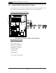
X7DVA-8/X7DVA-E User's Manual
LAN1
®
S
UPER X7DVA
SCSI Chan. A
IDE1
Fan4
SCSI Chan. B
PCI 33 MHz
JD1
GLAN
CTRLR
North Bridge
COM1
ATX PWR
8-Pin PWR
24-Pin
CPU2
South
Bridge
Fan1
SATA1
Slot1
Slot2
Slot3
PCI-Exp. x8
ZCR
JPL2
Slot5
DIMM 1A (Bank 1)
DIMM 1B (Bank 1)
DIMM 1C (Bank 1)
DIMM 2A (Bank 2)
DIMM 2B (Bank 2)
DIMM 2C (Bank 2)
JBT1
KB/
Mouse
USB 0/1
5000V
BIOS
LAN2
Fan6
JPWF
JAR
PWR I
2
C
VGA
PCI-X 100 MHz
(Green Slot)
JPG1
JWD
Printer
JPL1
JI
2
C1
JI
2
C2
JWOR
Floppy
JWOL
Fan2
CPU1
LE2
LE3
LE1
USB4/5
USB2/3
JPF
Buzzer
ESB2
VGA
CTRLR
SGPIO1
SGPIO2
JL1
VGA
Memory
S I/O
COM2
J2
J8B1
J7B3
J7B2
J7B1
J1
Battery
Slot6
SIM_LP
IPMI
PCI-Exp. x4
PCI-X 100 MHz
JPA1
SCSI
CTRLR
SATA0
SATA3
SATA2
SATA5
SATA4
JPA2
JPA3
JP1
JF1
FP CNTLR
Fan3
LE4
LE5
Fan5
D31
Power LED
The Power LED connection is located
on pins 15 and 16 of JF1. Refer to the
table on the right for pin defi nitions.
NMI Button
The non-maskable interrupt button
header is located on pins 19 and 20
of JF1. Refer to the table on the right
for pin defi nitions.
Power Button
OH/Fan Fail LED
1
NIC1 LED
Reset Button
2
HDD LED
Power LED
Reset
PWR
Vcc
Vcc
Vcc
Vcc
Ground
Ground
1920
Vcc
X
Ground
NMI
X
Vcc
PWR Fail LED
NIC2 LED
NMI Button
Pin Defi nitions (JF1)
Pin# Defi nition
19 Control
20 Ground
Power LED
Pin Defi nitions (JF1)
Pin# Defi nition
15 +5V
16 Ground
C. Front Control Panel Pin Defi nitions
A. NMI
B. PWR LED
A
B