
Datasheet

1-6
PDSLA/PDSLE User’s Manual
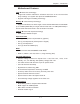
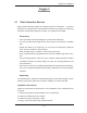
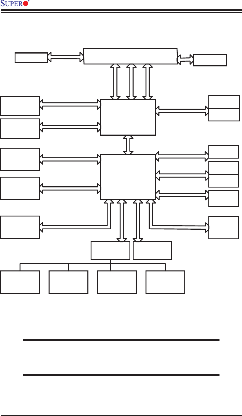
Figure 1-3. 945G/P Lakeport Chipset:
System Block Diagram
Note: This is a general block diagram and may not exactly represent
the features on your motherboard. See the following pages for the
actual specifi cations of each motherboard.
LAKEPORT
SLOTS
LGA775_PROCESSOR
ICH-7
USB
PORT_0~7
FWH
LPC I/O
MS.
KB. FDD. SER.1
SER.2
PRN.
PRI_IDE
VRM 10.1
ADDR
CTRL
DATA
UDMA/100
LPC
PCI_32_BUS
DDR2_667/533/400
VRM V10.1
DMI
4_PCI_x32
DIMM_CHA
S-ATA/300
4 x SATA
CK410 CLK
1 PCIE_x16
GRAPHIC
945G/P
DIMM_CHB
PORTS
PCIE_x16
INTEGRATED
GRAPHIC
82573 LAN
SLOTS
1_PCIE_x1
PCIE_x1
W83627HG 5.1-CH
AUDIO
FSB: 1066/800/533MHz
LPCUSB 2.0/1.1
AC97
PCIE_x1
1_PCIE_x8
SLOTS
(945G only)